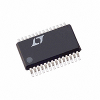
LTC3728LEGN-1#PBF Linear Technology, LTC3728LEGN-1#PBF Datasheet - Page 8

LTC3728LEGN-1#PBF
Manufacturer Part Number
LTC3728LEGN-1#PBF
Description
IC REG SYNC DUAL 28-SSOP
Manufacturer
Linear Technology
Series
PolyPhase®r
Type
Step-Down (Buck)r
Datasheet
1.LTC3728LEGN-1PBF.pdf
(32 pages)
Specifications of LTC3728LEGN-1#PBF
Internal Switch(s)
No
Synchronous Rectifier
Yes
Number Of Outputs
2
Voltage - Output
0.8 ~ 7 V
Current - Output
3A
Frequency - Switching
250kHz ~ 550kHz
Voltage - Input
4.5 ~ 28 V
Operating Temperature
-40°C ~ 85°C
Mounting Type
Surface Mount
Package / Case
28-SSOP
Lead Free Status / RoHS Status
Lead free / RoHS Compliant
Power - Output
-
Available stocks
Company
Part Number
Manufacturer
Quantity
Price
PIN FUNCTIONS
LTC3728L-1
V
Receives the remotely-sensed feedback voltage for each
controller from an external resistive divider across the
output.
PLLFLTR: Filter Connection for Phase-Locked Loop. Alter-
natively, this pin can be driven with an AC or DC voltage
source to vary the frequency of the internal oscillator.
PLLIN: External Synchronization Input to Phase Detector.
This pin is internally terminated to SGND with 50kΩ. The
phase-locked loop will force the rising top gate signal of
controller 1 to be synchronized with the rising edge of
the PLLIN signal.
FCB: Forced Continuous Control Input. This input acts
on both controllers and is normally used to regulate a
secondary winding. Pulling this pin below 0.8V will force
continuous synchronous operation.
I
Compensation Point. Each associated channels’ current
comparator trip point increases with this control voltage.
SGND: Small Signal Ground. Common to both controllers,
this pin must be routed separately from high current
grounds to the common (–) terminals of the C
capacitors.
3.3V
10mA DC with peak currents as high as 50mA.
NC: No Connect.
SENSE2
rent Comparators.
SENSE2
Comparators. The I
between the SENSE
R
RUN/SS2, RUN/SS1: Combination of soft-start and run
control inputs. A capacitor to ground at each of these pins
sets the ramp time to full output current. Forcing either of
these pins back below 1.0V causes the IC to shut down
the circuitry required for that particular controller.
8
TH1,
OSENSE1
SENSE
OUT
I
TH2
set the current trip threshold.
+
: Linear Regulator Output. Capable of supplying
–
: Error Amplifi er Output and Switching Regulator
, SENSE1
, V
, SENSE1
OSENSE2
+
–
–
: The (+) Input to the Differential Current
TH
: The (–) Input to the Differential Cur-
and SENSE
: Error Amplifi er Feedback Input.
pin voltage and controlled offsets
+
pins in conjunction with
OUT
TG2, TG1: High Current Gate Drives for Top N-Channel
MOSFETs. These are the outputs of fl oating drivers with
a voltage swing equal to INTV
the switch node voltage SW.
SW2, SW1: Switch Node Connections to Inductors. Voltage
swing at these pins is from a Schottky diode (external)
voltage drop below ground to V
BOOST2, BOOST1: Bootstrapped Supplies to the Top
Side Floating Drivers. Capacitors are connected between
the boost and switch pins and Schottky diodes are tied
between the boost and INTV
boost pins is from INTV
BG2, BG1: High Current Gate Drives for Bottom (Synchro-
nous) N-Channel MOSFETs. Voltage swing at these pins
is from ground to INTV
PGND: Driver Power Ground. Connects to the sources of
bottom (synchronous) N-channel MOSFETs, anodes of the
Schottky rectifi ers and the (–) terminal(s) of C
INTV
Regulator and the EXTV
circuits are powered from this voltage source. Must be
decoupled to power ground with a minimum of 4.7μF
tantalum or other low ESR capacitor.
EXTV
nected to INTV
power, bypassing the internal low dropout regulator, when-
ever EXTV
in Applications section. Do not exceed 7V on this pin.
V
between this pin and the signal ground pin.
PGOOD: Open-Drain Logic Output. PGOOD is pulled to
ground when the voltage on either V
within ±7.5% of its set point.
Exposed Pad (UH Package Only): Signal Ground. Must
be soldered to the PCB, providing a local ground for the
control components of the IC, and be tied to the PGND
pin under the IC.
IN
: Main Supply Pin. A bypass capacitor should be tied
CC
CC
: Output of the Internal 5V Linear Low Dropout
: External Power Input to an Internal Switch Con-
CC
is higher than 4.7V. See EXTV
CC
. This switch closes and supplies V
CC
CC
CC
.
Switch. The driver and control
to (V
CC
CC
pins. Voltage swing at the
IN
– 0.5V superimposed on
IN
.
+ INTV
OSENSE
CC
CC
).
connection
IN
pin is not
.
3728l1fc
CC


