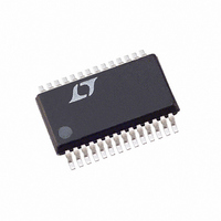
LTC3728LEGN-1#PBF Linear Technology, LTC3728LEGN-1#PBF Datasheet - Page 19

LTC3728LEGN-1#PBF
Manufacturer Part Number
LTC3728LEGN-1#PBF
Description
IC REG SYNC DUAL 28-SSOP
Manufacturer
Linear Technology
Series
PolyPhase®r
Type
Step-Down (Buck)r
Datasheet
1.LTC3728LEGN-1PBF.pdf
(32 pages)
Specifications of LTC3728LEGN-1#PBF
Internal Switch(s)
No
Synchronous Rectifier
Yes
Number Of Outputs
2
Voltage - Output
0.8 ~ 7 V
Current - Output
3A
Frequency - Switching
250kHz ~ 550kHz
Voltage - Input
4.5 ~ 28 V
Operating Temperature
-40°C ~ 85°C
Mounting Type
Surface Mount
Package / Case
28-SSOP
Lead Free Status / RoHS Status
Lead free / RoHS Compliant
Power - Output
-
Available stocks
Company
Part Number
Manufacturer
Quantity
Price
APPLICATIONS INFORMATION
stage is biased with internal resistors from an internal 2.4V
source as shown in the Functional Diagram. This requires
that current either be sourced or sunk from the SENSE
pins depending on the output voltage. If the output voltage
is below 2.4V current will fl ow out of both SENSE pins to
the main output. The output can be easily preloaded by
the V
comparator’s negative input bias current. The maximum
current fl owing out of each pair of SENSE pins is:
Since V
we can choose R1 in Figure 2 to have a maximum value
to absorb this current.
Regulating an output voltage of 1.8V, the maximum value
of R1 should be 32k. Note that for an output voltage above
2.4V, R1 has no maximum value necessary to absorb the
sense currents; however, R1 is still bounded by the V
feedback current.
Soft-Start/Run Function
The RUN/SS1 and RUN/SS2 pins are multipurpose pins that
provide a soft-start function and a means to shut down the
LTC3728L-1. Soft-start reduces the input power source’s
surge currents by gradually increasing the controller’s
current limit (proportional to V
used for power supply sequencing.
An internal 1.2μA current source charges up the C
tor
the particular controller is permitted to start operating. As
the voltage on RUN/SS increases from 1.5V to 3.0V, the
internal current limit is increased from 25mV/R
75mV/R
.
I
for V
R1
When the voltage on RUN/SS1 (RUN/SS2) reaches 1.5V,
SENSE
OUT
(MAX)
OUT
OSENSE
SENSE
+
resistive divider to compensate for the current
+ I
= 24k
< 2.4V
SENSE
. The output current limit ramps up slowly,
is servoed to the 0.8V reference voltage,
–
2.4V – V
= (2.4V – V
0.8V
OUT
ITH
OUT
). This pin can also be
)/24k
SS
SENSE
capaci-
OSENSE
to
taking an additional 1.25s/μF to reach full current. The
output current thus ramps up slowly, reducing the start-
ing surge current required from the input power supply.
If RUN/SS has been pulled all the way to ground there is
a delay before starting of approximately:
By pulling both RUN/SS pins below 1V, the IC is put into
low current shutdown (I
can be driven directly from logic as shown in Figure 7.
Diode D1 in Figure 7 reduces the start delay but allows
C
Each RUN/SS pin has an internal 6V zener clamp (See
Functional Diagram). Because the LTC3728L-1 is designed
for applications not requiring over current latchoff, no
pull-up resistor is required on the RUN/SS pin to defeat
latchoff. Refer to the LTC3728L/LTC3728LX datasheet if
this feature is required.
Fault Conditions: Current Limit and Current Foldback
The current comparators have a maximum sense volt-
age of 75mV resulting in a maximum MOSFET current
of 75mV/R
generally occurs with the largest V
3.3V OR 5V
SS
t
t
DELAY
IRAMP
to ramp up slowly providing the soft-start function.
D1
=
=
SENSE
(a)
1.2μA
3V 1.5V
1.5V
Figure 7. RUN/SS Pin Interfacing
1.2μA
. The maximum value of current limit
RUN/SS
C
SS
C
C
= 1.25s / μF
SS
SS
(
Q
= 1.25s / μF
= 20μA). The RUN/SS pins
(
LTC3728L-1
IN
at the highest ambi-
)
C
SS
)
C
(b)
SS
RUN/SS
19
3728L1 F07
3728l1fc
C
SS


