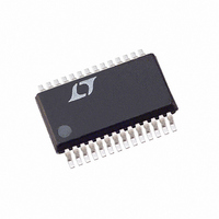
LTC3728LEGN-1#PBF Linear Technology, LTC3728LEGN-1#PBF Datasheet - Page 25

LTC3728LEGN-1#PBF
Manufacturer Part Number
LTC3728LEGN-1#PBF
Description
IC REG SYNC DUAL 28-SSOP
Manufacturer
Linear Technology
Series
PolyPhase®r
Type
Step-Down (Buck)r
Datasheet
1.LTC3728LEGN-1PBF.pdf
(32 pages)
Specifications of LTC3728LEGN-1#PBF
Internal Switch(s)
No
Synchronous Rectifier
Yes
Number Of Outputs
2
Voltage - Output
0.8 ~ 7 V
Current - Output
3A
Frequency - Switching
250kHz ~ 550kHz
Voltage - Input
4.5 ~ 28 V
Operating Temperature
-40°C ~ 85°C
Mounting Type
Surface Mount
Package / Case
28-SSOP
Lead Free Status / RoHS Status
Lead free / RoHS Compliant
Power - Output
-
Available stocks
Company
Part Number
Manufacturer
Quantity
Price
APPLICATIONS INFORMATION
Design Example
As a design example for one channel, assume V
12V(nominal), V
and f = 300kHz.
The inductance value is chosen fi rst based on a 30% ripple
current assumption. The highest value of ripple current
occurs at the maximum input voltage. Tie the PLLFLTR
pin to a resistive divider from the INTV
0.7V for 300kHz operation. The minimum inductance for
30% ripple current is:
or 3.7μH. Using standard inductor values:
A 4.7μH inductor will produce 23% ripple current and a
3.3μH will result in 33%. The peak inductor current will be
the maximum DC value plus one half the ripple current, or
5.84A, for the 3.3μH value. Increasing the ripple current
will also help ensure that the minimum on-time of 100ns
is not violated. The minimum on-time occurs at maximum
V
The R
maximum current sense voltage specifi cation with some
accommodation for tolerances:
Since the output voltage is below 2.4V the output resistive
divider will need to be sized to not only set the output
voltage but also to absorb the SENSE pin’s specifi ed
input current.
IN
L
R
t
:
ON(MIN)
SENSE
I
L
SENSE
(f)(I
V
=
IN
(f)(L)
V
RIPPLE
– V
OUT
=
resistor value can be calculated by using the
5.84A
60mV
OUT
V
IN(MAX)
V
1–
IN
)
OUT
•
= 22V(max), V
V
V
V
V
OUT
OUT
0.01
IN
IN
f
=
22V(300kHz)
1.8V
OUT
= 1.8V, I
CC
= 273ns
pin, generating
MAX
= 5A,
IN
=
Choosing 1% resistors: R1 = 25.5k and R2 = 32.4k yields
an output voltage of 1.816V.
The power dissipation on the top side MOSFET can be easily
estimated. Choosing a Fairchild FDS6982S dual MOSFET
results in: R
maximum input voltage with T(estimated) = 50°C:
A short-circuit to ground will result in a folded back
current of:
with a typical value of R
The resulting power dissipated in the bottom MOSFET is:
which is less than under full-load conditions.
C
temperature assuming only this channel is on. C
chosen with an ESR of 0.02Ω for low output ripple. The
output ripple in continuous mode will be highest at the
IN
R1
P
I
P
(
SC
is chosen for an RMS current rating of at least 3A at
0.035
MAIN
SYNC
5 – 2.3
(MAX)
=
1
0.01
25mV
=
=
= 100mW
= 24k
= 24k
1.8V
22V – 1.8V
DS(ON)
22V
+
)
+ 22V
2.3
(
1
22V
–
( )
5
2
1
= 0.035Ω/0.022Ω, C
2.4V – V
2.4V – 1.8V
(
300kHz
2
)
120ns(22V)
[
2
DS(ON)
1+ (0.005)(50°C – 25°C)
0.8V
0.8V
(
3.3μH
5A
2.1A
2
OUT
)
and δ = (0.005/°C)(20) = 0.1.
= 332mW
( )
)
2
4
(
1.125
LTC3728L-1
= 32k
(
= 2.1A
215pF
)
MILLER
(
0.022
)
•
= 215pF . At
]
•
)
25
OUT
3728l1fc
is


