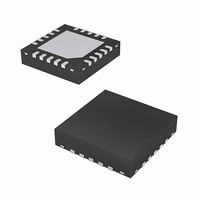
EL7520ILZ-T13 Intersil, EL7520ILZ-T13 Datasheet

EL7520ILZ-T13
Specifications of EL7520ILZ-T13
Related parts for EL7520ILZ-T13
EL7520ILZ-T13 Summary of contents
Page 1
... PART NUMBER PACKAGE TAPE & (NOTE) (Pb-FREE) EL7520ILZ 20 Ld 4x4 QFN EL7520ILZ- 4x4 QFN EL7520ILZ-T13 20 Ld 4x4 QFN EL7520AILZ 20 Ld 4x4 QFN EL7520AILZ- 4x4 QFN EL7520AILZ-T13 20 Ld 4x4 QFN NOTE: Intersil Pb-free plus anneal products employ special Pb-free material sets; molding compounds/die attach materials and 100% matte tin plate termination finish, which are RoHS compliant and compatible with both SnPb and Pb-free soldering operations ...
Page 2
Absolute Maximum Ratings ( ...
Page 3
Electrical Specifications 40°C to 85°C, unless otherwise specified. (Continued) PARAMETER DESCRIPTION ∆V /∆I Load Regulation DRVP Sink Current DRVP I DRVP Leakage Current L_DRVP V LDO OFF V FBN ...
Page 4
Typical Performance Curves 100 500 I (mA) OUT FIGURE 1. V EFFICIENCY vs I BOOST 0 -0.5 -1 -1 (V) ...
Page 5
Typical Performance Curves 0 -0.2 -0.4 -0.6 -0.8 -1 -1.2 -1 (mA) OUT FIGURE 7. V LOAD REGULATION OFF V CDLY EN V LOGIC V REF TIME (20ms/DIV) FIGURE 9. EL7520 START-UP SEQUENCE V BOOST ...
Page 6
Typical Performance Curves V CDLY EN V LOGIC V REF TIME (20ms/DIV) FIGURE 13. EL7520A START-UP SEQUENCE V BOOST V LOGIC V OFF V ON TIME (20ms/DIV) FIGURE 15. EL7520A START-UP SEQUENCE 6 EL7520, EL7520A (Continued BOOST V ...
Page 7
Typical Performance Curves 0.5µs/DIV FIGURE 18. LX WAVEFORM-CONTINUOUS MODE CH1=V , 100mV/DIV BOOST CH4=LOAD CURRENT, 200mA/DIV 0.2ms/DIV FIGURE 20. V TRANSIENT RESPONSE BOOST CH1=V , 100mV/DIV ON CH4=LOAD CURRENT, 50mA/DIV 50µs/DIV FIGURE 22. V TRANSIENT RESPONSE ON 7 EL7520, EL7520A ...
Page 8
Pin Descriptions PIN NUMBER PIN NAME 1 CDLY With a capacitor connected from this pin to GND sets the delay time for start-up sequence and sets the fault timeout time 2 DRVB Gate driver output for the external N channel ...
Page 9
Typical Application NODE 1000pF 500kΩ 0.1µF 0.1µ 10Ω 4.7µ 10K V REF C 41 0.1µF 0.1µF NODE 500Ω ...
Page 10
V REFERENCE REF GENERATOR FBB GM AMPLIFIER C INT UVLO COMPARATOR EN THERMAL SHUTDOWN DRVN BUFFER FBN 0.4V COMPARATOR Boost Converter The main boost converter is a current mode PWM controller operating at a fixed frequency. The 1MHz switching frequency ...
Page 11
V REF REFERENCE GENERATOR GM AMPLIFIER UVLO COMPARATOR FIGURE 25. FUNCTION DIAGRAM OF THE BOOST CONTROLLER The internal current limit circuitry is shown in Figure 26. The circuit senses the voltage across the R MOSFET is on; then compare it ...
Page 12
Input Capacitor The input capacitor is used to supply the current to the converter recommended that C IN The reflected ripple voltage will be smaller with larger C The voltage rating of input capacitor should be larger than ...
Page 13
The minimum base-emitter resistor, R calculated as: R _min = V _max/(I_DRVL_min - Ic/Hfe_min 1.25V/(8mA - 500mA/100) = 417Ω This is the minimum value that can be used - so, we now choose a convenient value greater ...
Page 14
Typical V voltage supported by EL7520, EL7520A range from LOGIC +1. -0.2V. A fault comparator is also included for DD monitoring the output voltage. The undervoltage threshold is set ...
Page 15
EL7520, EL7520A V CDLY EN V REF V BOOST LOGIC V OFF t DEL1 DELAYED V BOOST V ON START-UP SEQUENCE TIMED BY C FIGURE 30. EL7520 START-UP SEQUENCE DEL2 DLY FN7318.0 July ...
Page 16
EL7520, EL7520A V CDLY REF V BOOST LOGIC V OFF t DEL1 DELAYED V BOOST V ON START-UP SEQUENCE TIMED BY C FIGURE 31. EL7520A START-UP SEQUENCE DEL2 t ...
Page 17
Over-Temperature Protection An internal temperature sensor continuously monitor the die temperature. In the event that the die temperature exceeds the thermal trip point, the device will shut down. The upper and lower trigger points are typically set to 130°C and ...
Page 18
... Accordingly, the reader is cautioned to verify that data sheets are current before placing orders. Information furnished by Intersil is believed to be accurate and reliable. However, no responsibility is assumed by Intersil or its subsidiaries for its use; nor for any infringements of patents or other rights of third parties which may result from its use ...


