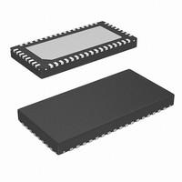
ISL65426IRZA-TS2698 Intersil, ISL65426IRZA-TS2698 Datasheet - Page 19

ISL65426IRZA-TS2698
Manufacturer Part Number
ISL65426IRZA-TS2698
Description
IC REG DUAL SYNC BUCK 6A 50-QFN
Manufacturer
Intersil
Type
Step-Down (Buck)r
Datasheet
1.ISL65426HRZ.pdf
(22 pages)
Specifications of ISL65426IRZA-TS2698
Internal Switch(s)
Yes
Synchronous Rectifier
Yes
Number Of Outputs
2
Voltage - Output
1 ~ 4 V
Current - Output
6A
Frequency - Switching
1MHz
Voltage - Input
3 ~ 5.5 V
Operating Temperature
-40°C ~ 85°C
Mounting Type
Surface Mount
Package / Case
50-VQFN
Lead Free Status / RoHS Status
Lead free / RoHS Compliant
Power - Output
-
regulator response, the output voltage initially deviates by an
amount shown in Equation 4.
The filter capacitors selected must have sufficiently low ESL
and ESR so that the total output voltage deviation ΔV is less
than the maximum allowable ripple.
The recommended load capacitance can be estimated using
Equation 5.
The internal compensation scheme assumes low-ESR
output capacitors. It is recommended to only use specialty
polymer or ceramic capacitors with ESRs of 10mΩ or lower.
Care also needs to be taken to ensure that the dielectric of
the capacitor used will work reliably in the entire temperature
range of the application.
Design Example:
Consider an output voltage of 1.2V, with LX1, LX2, LX3 and
LX4 connected. The output capacitance required would be:
C
A 330µF specialty polymer capacitor in parallel with three
47µF X7R ceramic capacitors would be the recommended
choice of output filter.
OUTPUT INDUCTOR SELECTION
Once the output capacitors are selected, the maximum
allowable ripple voltage, V
on the inductance. See Equation 7.
Since the output capacitors are supplying a decreasing
portion of the load current while the regulator recovers from
the transient, the capacitor voltage becomes slightly
depleted. The output inductors must be capable of assuming
the entire load current before the output voltage decreases
more than ΔV
Equation 8 gives the upper limit on output inductance for the
cases when the trailing edge of the current transient causes
the greater output voltage deviation than the leading edge.
Equation 9 addresses the leading edge. Normally, the
trailing edge dictates the inductance selection because duty
cycles are usually less than 50%. Nevertheless, both
inequalities should be evaluated, and inductance should be
governed based on the lower of the two results. In each
equation, L is the output inductance and C is the total output
capacitance.
ΔV
L
C
OUT
OUT
≥
≈
ESR
ESL
=
=
×
0.5 4 150μF
0.5
×
(
---------------------------------------------------- -
f
V
•
s
di
---- -
dt
×
IN
×
MAX
Number of LX channels used
•
V
+
–
IN
[
V
ESR
. This places an upper limit on inductance.
OUT
×
V
PP
)V
×
•
ΔI
1.8V
------------
1.2V
MAX
OUT
PPMAX
]
19
=
450μF
, determines the lower limit
×
150μF
×
--------------- -
V
1.8V
OUT
(EQ. 4)
(EQ. 5)
(EQ. 6)
(EQ. 7)
ISL65426
The other concern when selecting an output inductor is the
internally set current mode slope compensation. Designs
should not allow inductor ripple currents below 0.125 times
the maximum output current to prevent regulation issues.
It is recommended to use a 30% peak-to-peak ripple current
value to calculate out the inductance required for the
application. Accordingly, the inductance estimated using
Equation 10 below would fall between the minimum
inductance value calculated in Equation 7 and the maximum
values determined from Equations 8 and 9.
Input Capacitor Selection
Input capacitors are responsible for sourcing the AC
component of the input current flowing into the switching
power devices. Their RMS current capacity must be
sufficient to handle the AC component of the current drawn
by the switching power devices, which is related to duty
cycle. The maximum RMS current required by the regulator
is closely approximated by Equation 11.
The important parameters to consider when selecting an
input capacitor are the voltage rating and the RMS current
rating. For reliable operation, select capacitors with voltage
ratings above the maximum input voltage. The rated voltage
rating should be at least 1.25 times greater than the
maximum input voltage while using aluminum electrolytic
capacitors, and about 2 times the maximum input voltage to
account for capacitance derating in case of ceramic
capacitors. The capacitor RMS current rating should be
higher than the largest RMS current required by the circuit.
The ISL65426 needs a minimum effective input capacitance
of 70µF with low ESR for stable operation.
Layout Considerations
Careful printed circuit board (PCB) layout is critical in high
frequency switching converter design. Current transitions
from one device to another at this frequency induce voltage
spikes across the interconnecting impedances and parasitic
elements. These spikes degrade efficiency, lead to device
overvoltage stress, radiate noise into sensitive nodes, and
increase thermal stress on critical components. Careful
component placement and PCB layout minimizes the
voltage spikes in the converter.
L
L
L
I
RMS
@
≤
≤
2 C V
------------------------ - ΔV
(
------------------------ - ΔV
1.25
(
--------------------------------------------------------------- -
⋅
(
(
V IN V OUT
V IN
MAX
ΔI
ΔI
⋅
)
) C
)
2
2
–
×
⋅
O
f s
=
×
V
-----------------
I
---------------------------- -
OUT
V
OUT
MAX
)
MAX
IN
×
3
V OUT
MAX
×
–
–
⎛
⎜
⎝
(
(
I
ΔI ESR
ΔI ESR
OUT
⋅
⋅
MAX
)
)
2
+
⎛
⎝
V
----- -
12
1
IN
×
–
⎛
⎜
⎝
V IN V OUT
--------------------------------- -
V
O
⎞
⎠
L
–
×
f
s
×
March 25, 2008
V
-----------------
V IN
OUT
(EQ. 10)
(EQ. 11)
(EQ. 8)
(EQ. 9)
FN6340.3
⎞ 2
⎟
⎠
⎞
⎟
⎠


