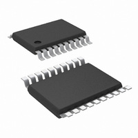
LM5118MH/NOPB National Semiconductor, LM5118MH/NOPB Datasheet - Page 13

LM5118MH/NOPB
Manufacturer Part Number
LM5118MH/NOPB
Description
IC CTLR BUCK-BOOST 20-TSSOP
Manufacturer
National Semiconductor
Series
PowerWise®r
Type
Step-Down (Buck), Step-Up (Boost)r
Datasheet
1.LM5118MHXNOPB.pdf
(26 pages)
Specifications of LM5118MH/NOPB
Internal Switch(s)
No
Synchronous Rectifier
Yes
Number Of Outputs
1
Voltage - Output
1.23 ~ 70 V
Frequency - Switching
500kHz
Voltage - Input
3 ~ 75 V
Operating Temperature
-40°C ~ 125°C
Mounting Type
Surface Mount
Package / Case
20-TSSOP Exposed Pad, 20-eTSSOP, 20-HTSSOP
Dc To Dc Converter Type
Step Up/Step Down
Pin Count
20
Input Voltage
3 to 75V
Output Voltage
1.23 to 70V
Output Current
3.5A
Package Type
TSSOP EP
Mounting
Surface Mount
Operating Temperature Classification
Automotive
Operating Temperature (min)
-40C
Operating Temperature (max)
125C
Package
20TSSOP EP
For Use With
LM5118EVAL - BOARD EVALUATION FOR LM5118
Lead Free Status / RoHS Status
Lead free / RoHS Compliant
Current - Output
-
Power - Output
-
Lead Free Status / Rohs Status
Compliant
Other names
LM5118MH
Available stocks
Company
Part Number
Manufacturer
Quantity
Price
Company:
Part Number:
LM5118MH/NOPB
Manufacturer:
ZARLINK
Quantity:
14
3V returns the regulator to normal operation. The EN pin can
be tied directly to the VIN pin if this function is not needed. It
must not be left floating. A 1 MΩ pull-up resistor to VIN can
be used to interface with an open collector or open drain con-
trol signal.
UVLO
An under-voltage lockout pin is provided to disable the regu-
lator when the input is below the desired operating range. If
the UVLO pin is below 1.13V, the regulator enters a standby
mode with the outputs disabled, but with VCC regulator op-
erating. If the UVLO input exceeds 1.23V, the regulator will
resume normal operation. A voltage divider from the input to
ground can be used to set a VIN threshold to disable the reg-
ulator in brown-out conditions or for low input faults.
If a current limit fault exists for more than 256 clock cycles,
the regulator will enter a “hiccup” mode of current limiting and
the UVLO pin will be pulled low by an internal switch. This
switch turns off when the UVLO pin approaches ground po-
tential allowing the UVLO pin to rise. A capacitor connected
to the UVLO pin will delay the return to a normal operating
level and thereby set the off-time of the hiccup mode fault
protection. An internal 5 µA pull-up current pulls the UVLO pin
to a high state to ensure normal operation when the VIN
UVLO function is not required and the pin is left floating.
Oscillator and Sync Capability
The LM5118 oscillator frequency is set by a single external
resistor connected between the RT pin and the AGND pin.
The R
connected directly to the pins of the IC. To set a desired os-
cillator frequency (f), the necessary value for the R
can be calculated from the following equation:
The SYNC pin can be used to synchronize the internal oscil-
lator to an external clock. The external clock must be of higher
T
resistor should be located very close to the device and
FIGURE 8. Simplified Oscillator and Block Diagram with Sync I/O Circuit
T
resistor
13
frequency than the free-running frequency set by the R
sistor. A clock circuit with an open drain output is the recom-
mended interface from the external clock to the SYNC pin.
The clock pulse duration should be greater than 15 ns.
Multiple LM5118 devices can be synchronized together sim-
ply by connecting the SYNC pins together. In this configura-
tion all of the devices will be synchronized to the highest
frequency device. The diagram in
SYNC input/output features of the LM5118. The internal os-
cillator circuit drives the SYNC pin with a strong pull-down/
weak pull-up inverter. When the SYNC pin is pulled low, either
by the internal oscillator or an external clock, the ramp cycle
of the oscillator is terminated and forced 400 ns off-time is
initiated before a new oscillator cycle begins. If the SYNC pins
of several LM5118 IC’s are connected together, the IC with
the highest internal clock frequency will pull all the connected
SYNC pins low and terminate the oscillator ramp cycles of the
other IC’s. The LM5118 with the highest programmed clock
frequency will serve as the master and control the switching
frequency of all the devices with lower oscillator frequencies.
FIGURE 7. Sync from Multiple Devices
30058519
Figure 7
30058518
illustrates the
www.national.com
T
re-


