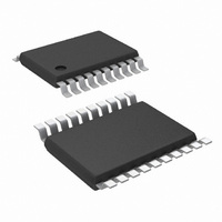
LM5118MH/NOPB National Semiconductor, LM5118MH/NOPB Datasheet - Page 15

LM5118MH/NOPB
Manufacturer Part Number
LM5118MH/NOPB
Description
IC CTLR BUCK-BOOST 20-TSSOP
Manufacturer
National Semiconductor
Series
PowerWise®r
Type
Step-Down (Buck), Step-Up (Boost)r
Datasheet
1.LM5118MHXNOPB.pdf
(26 pages)
Specifications of LM5118MH/NOPB
Internal Switch(s)
No
Synchronous Rectifier
Yes
Number Of Outputs
1
Voltage - Output
1.23 ~ 70 V
Frequency - Switching
500kHz
Voltage - Input
3 ~ 75 V
Operating Temperature
-40°C ~ 125°C
Mounting Type
Surface Mount
Package / Case
20-TSSOP Exposed Pad, 20-eTSSOP, 20-HTSSOP
Dc To Dc Converter Type
Step Up/Step Down
Pin Count
20
Input Voltage
3 to 75V
Output Voltage
1.23 to 70V
Output Current
3.5A
Package Type
TSSOP EP
Mounting
Surface Mount
Operating Temperature Classification
Automotive
Operating Temperature (min)
-40C
Operating Temperature (max)
125C
Package
20TSSOP EP
For Use With
LM5118EVAL - BOARD EVALUATION FOR LM5118
Lead Free Status / RoHS Status
Lead free / RoHS Compliant
Current - Output
-
Power - Output
-
Lead Free Status / Rohs Status
Compliant
Other names
LM5118MH
Available stocks
Company
Part Number
Manufacturer
Quantity
Price
Company:
Part Number:
LM5118MH/NOPB
Manufacturer:
ZARLINK
Quantity:
14
Where g
and A is the current sense amplifier gain (10V/V). The ramp
capacitor should be located very close to the device and con-
nected directly to the RAMP and AGND pins.
The relationship between the average inductor current and
the pedestal value of the sampled inductor current can cause
instability in certain operating conditions. This instability is
known as sub-harmonic oscillation, which occurs when the
inductor ripple current does not return to its initial value by the
start of the next switching cycle. Sub-harmonic oscillation is
normally characterized by observing alternating wide and nar-
row pulses at the switch node. Adding a fixed slope voltage
ramp (slope compensation) to the current sense signal pre-
vents this oscillation. The 50µA of offset current provided from
the emulated current source adds enough slope compensa-
tion to the ramp signal for output voltages less than or equal
to 12V. For higher output voltages, additional slope compen-
sation may be required. In such applications, the ramp ca-
pacitor can be decreased from the nominal calculated value
to increase the ramp slope compensation.
The pedestal current sample is obtained from the current
sense resistor (Rs) connected to the CS and CSG pins. It is
sometimes helpful to adjust the internal current sense ampli-
fier gain (A) to a lower value in order to obtain the higher
current limit threshold. Adding a pair of external resistors RG
in a series with CS and CSG as shown in
the current sense amplifier gain A according to the following
equation:
m
is the ramp generator transconductance (5 µA/V)
FIGURE 10. Current Limit and Ramp Circuit
Figure 10
reduces
15
Current Limit
In the buck mode the average inductor current is equal to the
output current (Iout). In buck-boost mode the average induc-
tor current is approximately equal to:
Consequently, the inductor current in buck-boost mode is
much larger especially when VOUT is large relative to VIN.
The LM5118 provides a current monitoring scheme to protect
the circuit from possible over-current conditions. When set
correctly, the emulated current sense signal is proportional to
the buck switch current with a scale factor determined by the
current sense resistor. The emulated ramp signal is applied
to the current limit comparator. If the peak of the emulated
ramp signal exceeds 1.25V when operating in the buck mode,
the PWM cycle is immediately terminated (cycle-by-cycle cur-
rent limiting). In buck-boost mode the current limit threshold
is increased to 2.50V to allow higher peak inductor current.
To further protect the external switches during prolonged
overload conditions, an internal counter detects consecutive
cycles of current limiting. If the counter detects 256 consec-
utive current limited PWM cycles, the LM5118 enters a low
power dissipation hiccup mode. In the hiccup mode, the out-
put drivers are disabled, the UVLO pin is momentarily pulled
low, and the soft-start capacitor is discharged. The regulator
is restarted with a normal soft-start sequence once the UVLO
pin charges back to 1.23V. The hiccup mode off-time can be
programmed by an external capacitor connected from UVLO
pin to ground. This hiccup cycle will repeat until the output
overload condition is removed.
In applications with low output inductance and high input volt-
age, the switch current may overshoot due to the propagation
delay of the current limit comparator and control circuitry. If
an overshoot should occur, the sample-and-hold circuit will
detect the excess re-circulating diode current. If the sample-
and-hold pedestal level exceeds the internal current limit
threshold, the buck switch will be disabled and will skip PWM
cycles until the inductor current has decayed below the cur-
rent limit threshold. This approach prevents current runaway
conditions due to propagation delays or inductor saturation
since the inductor current is forced to decay before the buck
switch is turned on again.
30058523
www.national.com


