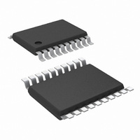
LM5118MH/NOPB National Semiconductor, LM5118MH/NOPB Datasheet - Page 16

LM5118MH/NOPB
Manufacturer Part Number
LM5118MH/NOPB
Description
IC CTLR BUCK-BOOST 20-TSSOP
Manufacturer
National Semiconductor
Series
PowerWise®r
Type
Step-Down (Buck), Step-Up (Boost)r
Datasheet
1.LM5118MHXNOPB.pdf
(26 pages)
Specifications of LM5118MH/NOPB
Internal Switch(s)
No
Synchronous Rectifier
Yes
Number Of Outputs
1
Voltage - Output
1.23 ~ 70 V
Frequency - Switching
500kHz
Voltage - Input
3 ~ 75 V
Operating Temperature
-40°C ~ 125°C
Mounting Type
Surface Mount
Package / Case
20-TSSOP Exposed Pad, 20-eTSSOP, 20-HTSSOP
Dc To Dc Converter Type
Step Up/Step Down
Pin Count
20
Input Voltage
3 to 75V
Output Voltage
1.23 to 70V
Output Current
3.5A
Package Type
TSSOP EP
Mounting
Surface Mount
Operating Temperature Classification
Automotive
Operating Temperature (min)
-40C
Operating Temperature (max)
125C
Package
20TSSOP EP
For Use With
LM5118EVAL - BOARD EVALUATION FOR LM5118
Lead Free Status / RoHS Status
Lead free / RoHS Compliant
Current - Output
-
Power - Output
-
Lead Free Status / Rohs Status
Compliant
Other names
LM5118MH
Available stocks
Company
Part Number
Manufacturer
Quantity
Price
Company:
Part Number:
LM5118MH/NOPB
Manufacturer:
ZARLINK
Quantity:
14
www.national.com
Maximum Duty Cycle
Each conduction cycle of the buck switch is followed by a
forced minimum off-time of 400ns to allow sufficient time for
the re-circulating diode current to be sampled. This forced off-
time limits the maximum duty cycle of the controller. The
actual maximum duty cycle will vary with the operating fre-
quency as follows:
where f is the oscillator frequency in Hz
Limiting the maximum duty cycle will limit the maximum boost
ratio (VOUT/VIN) while operating in buck-boost mode. For
example, from
kHz, D
With D= 80%, solving for VOUT results in,
VOUT = 4 x VIN
With a minimum input voltage of 5 volts, the maximum pos-
sible output voltage is 20 volts at f = 500 kHz. The buck-boost
step-up ratio can be increased by reducing the operating fre-
quency which increases the maximum duty cycle.
Soft-Start
The soft-start feature allows the regulator to gradually reach
the initial steady state operating point, thus reducing start-up
stresses and surges. The internal 10 µA soft-start current
source gradually charges an external soft-start capacitor con-
nected to the SS pin. The SS pin is connected to the positive
input of the internal error amplifier. The error amplifier controls
the pulse-width modulator such that the FB pin approximately
equals the SS pin as the SS capacitor is charged. Once the
SS pin voltage exceeds the internal 1.23V reference voltage,
the error amp is controlled by the reference instead of the SS
pin. The SS pin voltage is clamped by an internal amplifier at
a level of 150 mV above the FB pin voltage. This feature pro-
vides a soft-start controlled recovery in the event a severe
overload pulls the output voltage (and FB pin) well below nor-
mal regulation but doesn’t persist for 256 clock cycles.
FIGURE 11. Maximum Duty Cycle vs Frequency
MAX
is 80%. Using the buck-boost transfer function.
Figure
D
MAX
11, at an operating frequency of 500
= 1 - f x 400 x 10
-9
30058526
16
Various sequencing and tracking schemes can be imple-
mented using external circuits that limit or clamp the voltage
level of the SS pin. The SS pin acts as a non-inverting input
to the error amplifier anytime SS voltage is less than the 1.23V
reference. In the event a fault is detected (over-temperature,
VCC under-voltage, hiccup current limit), the soft-start ca-
pacitor will be discharged. When the fault condition is no
longer present, a new soft-start sequence will begin.
HO Ouput
The LM5118 contains a high side, high current gate driver and
associated high voltage level shift. This gate driver circuit
works in conjunction with an internal diode and an external
bootstrap capacitor. A 0.1 µF ceramic capacitor, connected
with short traces between the HB pin and HS pin is recom-
mended for most circuit configurations. The size of the boot-
strap capacitor depends on the gate charge of the external
FET. During the off time of the buck switch, the HS pin voltage
is approximately -0.5V and the bootstrap capacitor is charged
from VCC through the internal bootstrap diode. When oper-
ating with a high PWM duty cycle, the buck switch will be
forced off each cycle for 400ns to ensure that the bootstrap
capacitor is recharged.
Thermal Protection
Internal Thermal Shutdown circuitry is provided to protect the
integrated circuit in the event the maximum junction temper-
ature is exceeded. When activated, typically at 165°C, the
controller is forced into a low power reset state, disabling the
output driver and the bias regulator. This protection is provid-
ed to prevent catastrophic failures from accidental device
overheating.
Application Information
The procedure for calculating the external components is il-
lustrated with the following design example. The designations
used in the design example correlate to the final schematic
shown in
•
•
•
•
•
R7 = R
RT sets the oscillator switching frequency. Generally speak-
ing, higher operating frequency applications will use smaller
components, but have higher switching losses. An operating
frequency of 300 kHz was selected for this example as a rea-
sonable compromise for both component size and efficiency.
The value of R
therefore, R7 = 18.3 kΩ
VOUT = 12V
VIN = 5V to 75V
F = 300 kHz
Minimum load current (CCM operation) = 600 mA
Maximum load current = 3A
T
Figure
T
can be calculated as follows:
18. The design specifications are:


