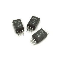
ACPL-W314-500E Avago Technologies US Inc., ACPL-W314-500E Datasheet - Page 5

ACPL-W314-500E
Manufacturer Part Number
ACPL-W314-500E
Description
OPTOCOUPLER IGBT 0.4A 6-SOIC
Manufacturer
Avago Technologies US Inc.
Specifications of ACPL-W314-500E
Output Type
Push-Pull, Totem-Pole
Package / Case
6-SOP
Voltage - Isolation
3750Vrms
Number Of Channels
1, Unidirectional
Current - Output / Channel
600mA
Propagation Delay High - Low @ If
300ns @ 7mA
Current - Dc Forward (if)
25mA
Input Type
DC
Mounting Type
Surface Mount
Fall Time
50 ns
Rise Time
50 ns
Configuration
1 Channel
Isolation Voltage
3750 Vrms
Maximum Propagation Delay Time
700 ns
Maximum Forward Diode Voltage
1.8 V
Minimum Forward Diode Voltage
1.2 V
Maximum Reverse Diode Voltage
5 V
Maximum Forward Diode Current
12 mA
Maximum Power Dissipation
250 mW
Maximum Operating Temperature
+ 100 C
Minimum Operating Temperature
- 40 C
Lead Free Status / RoHS Status
Lead free / RoHS Compliant
Available stocks
Company
Part Number
Manufacturer
Quantity
Price
Table 2. Insulation and Safety Related Specifications
Table 3. Absolute Maximum Ratings
Table 4. Recommended Operating Conditions
Notes:
1. Derate linearly above 70°C free air temperature at a rate of 0.3 mA/°C.
2. Maximum pulse width = 10 Ps, maximum duty cycle = 0.2%. This value is intended to allow for component tolerances for designs with I
3. Derate linearly above 85°C, free air temperature at the rate of 4.0 mW/°C.
4. Input power dissipation does not require derating.
5
Parameter
Minimum External Air Gap
(External Clearance)
Minimum External Tracking
(External Creepage)
Minimum Internal Plastic Gap
(Internal Clearance)
Minimum Internal Tracking
(Internal Creepage)
Tracking Resistance
(Comparative Tracking Index)
Isolation Group
Parameter
Storage Temperature
Operating Temperature
Average Input Current
Peak Transient Input Current
(<1 μs pulse width, 300pps)
Reverse Input Voltage
“High” Peak Output Current
“Low” Peak Output Current
Supply Voltage
Output Voltage
Output Power Dissipation
Input Power Dissipation
Lead Solder Temperature
Solder Reflow Temperature Profile
Parameter
Power Supply
Input Current (ON)
Input Voltage (OFF)
Operating Temperature
minimum = 0.4 A. See Application section for additional details on limiting I
Symbol
L(101)
L(102)
CTI
>175
P314
0.08
NA
7.0
8.0
IIIa
Symbol
T
T
I
I
V
I
I
V
V
P
P
260°C for 10 sec., 1.6 mm below seating plane
See Package Outline Drawings section
Symbol
V
I
V
T
ACPL-
F(AVG)
F(TRAN)
OH(PEAK)
OL(PEAK)
F(ON)
A
A
S
R
CC
O(PEAK)
O
I
CC
F(OFF)
- V
- V
W314
>175
0.08
8.0
8.0
NA
IIIa
EE
EE
Min.
-55
-40
-0.5
-0.5
Min.
10
8
- 3.6
- 40
Unit
mm
mm
mm
mm
OL
V
peak.
Conditions
Measured from input terminals to output termi-
nals, shortest distance through air.
Measured from input terminals to output termi-
nals, shortest distance path along body.
Through insulation distance conductor to con-
ductor, usually the straight line distance thick-
ness between the emitter and detector.
Measured from input terminals to output termi-
nals, along internal cavity.
DIN IEC 112/VDE 0303 Part 1
Material Group (DIN VDE 0110, 1/89, Table 1)
Max.
125
100
25
1.0
5
0.6
0.6
35
V
250
45
Max.
30
12
0.8
100
CC
Units
°C
°C
mA
A
V
A
A
V
V
mW
mW
Units
V
mA
V
°C
Note
1
2
2
3
4
Note
O
peak


