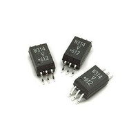
ACPL-W314-500E Avago Technologies US Inc., ACPL-W314-500E Datasheet - Page 6

ACPL-W314-500E
Manufacturer Part Number
ACPL-W314-500E
Description
OPTOCOUPLER IGBT 0.4A 6-SOIC
Manufacturer
Avago Technologies US Inc.
Specifications of ACPL-W314-500E
Output Type
Push-Pull, Totem-Pole
Package / Case
6-SOP
Voltage - Isolation
3750Vrms
Number Of Channels
1, Unidirectional
Current - Output / Channel
600mA
Propagation Delay High - Low @ If
300ns @ 7mA
Current - Dc Forward (if)
25mA
Input Type
DC
Mounting Type
Surface Mount
Fall Time
50 ns
Rise Time
50 ns
Configuration
1 Channel
Isolation Voltage
3750 Vrms
Maximum Propagation Delay Time
700 ns
Maximum Forward Diode Voltage
1.8 V
Minimum Forward Diode Voltage
1.2 V
Maximum Reverse Diode Voltage
5 V
Maximum Forward Diode Current
12 mA
Maximum Power Dissipation
250 mW
Maximum Operating Temperature
+ 100 C
Minimum Operating Temperature
- 40 C
Lead Free Status / RoHS Status
Lead free / RoHS Compliant
Available stocks
Company
Part Number
Manufacturer
Quantity
Price
Table 5. Electrical Specifications (DC)
Over recommended operating conditions unless otherwise specified.
Table 6. Switching Specifications (AC)
Over recommended operating conditions unless otherwise specified.
Notes:
1. Maximum pulse width = 50 Ps, maximum duty cycle = 0.5%.
2. Maximum pulse width = 10 Ps, maximum duty cycle = 0.2%. This value is intended to allow for component tolerances for designs with I
3. In this test, V
4. Maximum pulse width = 1 ms, maximum duty cycle = 20%.
5. The power supply current increases when operating frequency and Q
6. This load condition approximates the gate load of a 1200 V/25 A IGBT.
7. PDD is the difference between t
8. Common mode transient immunity in the high state is the maximum tolerable |dV
9. Common mode transient immunity in a low state is the maximum tolerable |dV
6
Parameter
High Level Output Current
Low Level Output Current
High Level Output Voltage
Low Level Output Voltage
High Level Supply Current
Low Level Supply Current
Threshold Input Current
Low to High
Threshold Input Voltage
High to Low
Input Forward Voltage
Temperature Coefficient of
Input Forward Voltage
Input Reverse Breakdown Voltage
Input Capacitance
Parameter
Propagation Delay Time
to High Output Level
Propagation Delay Time
to Low Output Level
Propagation Delay
Difference Between
Any Two Parts or Channels
Rise Time
Fall Time
Output High Level Common
Mode Transient Immunity
Output Low Level Common
Mode Transient Immunity
minimum = 0.4 A. See Application section for additional details on limiting I
output will remain in the high state (i.e. V
will remain in a low state (i.e. V
OH
is measured with a DC load current. When driving capacitive load V
O
PHL
< 1.0 V).
and t
Symbol
I
I
V
V
I
I
I
V
V
'V
BV
C
Symbol
t
t
PDD
t
t
|CM
|CM
PLH
O
OH
OL
CCH
CCL
FLH
PLH
PHL
R
F
OH
OL
FHL
F
IN
> 6.0 V).
R
F
between any two parts or channels under the same test conditions.
/'T
H
L
|
|
A
Min.
0.2
0.4
0.2
0.4
V
0.8
1.2
5
Min.
0.1
0.1
-0.5
25
25
CC
-4
Typ.
Typ.
0.5
0.4
0.5
V
0.4
0.7
1.2
1.5
-1.6
60
0.2
0.3
50
50
CC
-1.8
g
of the driven IGBT increases.
Max.
1
3
3
7
1.8
Max.
0.7
0.7
0.5
OL
CM
peak.
/dt| of the common mode pulse, V
OH
Units
Units
A
A
A
A
V
V
mA
mA
mA
V
V
mV/°C
V
pF
μs
μs
μs
ns
ns
kV/μs
kV/μs
CM
will approach V
/dt| of the common mode pulse V
Test Conditions
V
V
V
V
I
I
I
I
I
I
I
I
I
f = 1 MHz, V
Test Conditions
R
f = 10 kHz,
Duty Cycle = 50%,
I
T
V
O
O
F
F
O
O
F
F
R
F
A
g
O
O
O
O
CM
= 10 mA
= 0 mA
= 10 mA
= 10 mA
= 8 mA, V
= 10 μA
= 0 mA, V
= -100 mA
= 100 mA
= 0 mA, V
= 25°C,
= 47:, C
= V
= V
= V
= V
= 1500 V
CC
CC
CC
EE
EE
as I
+ 2.5
+ 10
- 4
- 10
OH
CC
g
O
O
F
= 0 V
= 3 nF,
> 5 V
> 5 V
approaches zero amps.
= 30 V
CM
, to assure that the output
CM
Fig.
2
3
5
6
1
4
7, 8
7, 8
9, 15
16
Fig.
10, 11,
12, 13,
14, 17
18
18
to assure that the
Note
1
2
1
2
3, 4
5
5
Note
6
6
7
8
9
O
peak


