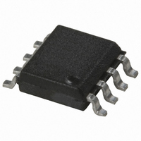
HCPL-0738-500 Avago Technologies US Inc., HCPL-0738-500 Datasheet - Page 5

HCPL-0738-500
Manufacturer Part Number
HCPL-0738-500
Description
OPTOCOUPLER 15MBD 2CH 8-SOIC
Manufacturer
Avago Technologies US Inc.
Datasheet
1.HCPL-0738-500.pdf
(8 pages)
Specifications of HCPL-0738-500
Package / Case
8-SOIC (0.154", 3.90mm Width)
Voltage - Isolation
3750Vrms
Number Of Channels
2, Unidirectional
Current - Output / Channel
2mA
Data Rate
15MBd
Propagation Delay High - Low @ If
35ns @ 12mA
Current - Dc Forward (if)
20mA
Input Type
DC
Output Type
Open Collector
Mounting Type
Surface Mount
Isolation Voltage
3750 Vrms
Maximum Continuous Output Current
2 mA
Maximum Fall Time
25 ns
Maximum Forward Diode Current
20 mA
Maximum Rise Time
20 ns
Minimum Forward Diode Voltage
1.3 V
Output Device
Logic Gate Photo IC
Configuration
2 Channel
Maximum Baud Rate
15 MBps
Maximum Forward Diode Voltage
1.8 V
Maximum Operating Temperature
+ 100 C
Minimum Operating Temperature
- 40 C
Lead Free Status / RoHS Status
Contains lead / RoHS non-compliant
Available stocks
Company
Part Number
Manufacturer
Quantity
Price
Company:
Part Number:
HCPL-0738-500E
Manufacturer:
AVAGO
Quantity:
300
Electrical Specifications
Over recommended temperature (T
All typical specifications are at T
Parameter
Input Forward Voltage
Input Reverse Breakdown
Voltage
Logic High Output Voltage
Logic Low Output Voltage
Input Threshold Current
Logic Low Output Supply
Current
Logic High Output Supply
Current
Switching Specifications
Over recommended temperature (T
All typical specifications are at T
Parameter
Propagation Delay Time
to Logic Low Output
Propagation Delay Time
to Logic High Output
Pulse Width
Pulse Width Distortion
Propagation Delay Skew
Output Rise Time
(10% – 90%)
Output Fall Time
(90% – 10%)
Common Mode Transient
Immunity at Logic High Output
Common Mode Transient
Immunity at Logic Low Output
5
A
A
= 5˚C, V
= 5˚C, V
A
A
= –0˚C to +100˚C) and .5 V ≤ V
= –0˚C to +100˚C) and .5 V ≤ V
Symbol
V
BV
V
V
I
I
I
TH
DDL
DDH
F
OH
OL
R
Symbol
t
t
PW
|PWD|
t
t
t
|CM
|CM
PHL
PLH
PSK
R
F
DD
DD
= +5 V.
= +5 V.
H
L
|
|
Min.
1.3
5
.0
Min.
0
11
100
0
10
10
Typ.
1.5
5
0.01
.5
10
8
Typ.
35
0
15
0
5
15
15
DD
DD
≤ 5.5 V.
≤ 5.5 V.
Max.
1.8
0.1
8.
18.0
15.0
Max.
60
60
30
0
Units
V
V
V
V
mA
mA
mA
Units
ns
ns
ns
ns
ns
ns
ns
kV/µS
kV/µS
Test Conditions
I
CMOS Signal Levels
I
CMOS Signal Levels
I
CMOS Signal Levels
I
CMOS Signal Levels
I
CMOS Signal Levels
I
CMOS Signal Levels
V
I
V
I
Test Conditions
I
I
I
I
I
I
I
F
F
F
F
F
F
F
F
F
R
F
F
OL
F
F
CM
CM
= 1 mA, C
= 1 mA, C
= 1 mA, C
= 1 mA, C
= 0 mA, C
= 1 mA, C
= 0 mA
= 1 mA
= 1 mA
= 0, I
= 1 mA, I
= 1 mA
= 0 mA
= 10 µA
= 0 µA
= 1000 V, T
= 1000 V, T
O
= –0 µA
L
= 15 pF
O
L
L
L
L
L
= 0 µA
= 15 pF
= 15 pF
= 15 pF
= 15 pF
= 15 pF
A
A
= 5˚C,
= 5˚C,
Fig.
1
3
Fig.
5
5
5
Notes
Notes
1
1
3
5


