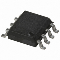
HCPL-0738-500 Avago Technologies US Inc., HCPL-0738-500 Datasheet - Page 8

HCPL-0738-500
Manufacturer Part Number
HCPL-0738-500
Description
OPTOCOUPLER 15MBD 2CH 8-SOIC
Manufacturer
Avago Technologies US Inc.
Datasheet
1.HCPL-0738-500.pdf
(8 pages)
Specifications of HCPL-0738-500
Package / Case
8-SOIC (0.154", 3.90mm Width)
Voltage - Isolation
3750Vrms
Number Of Channels
2, Unidirectional
Current - Output / Channel
2mA
Data Rate
15MBd
Propagation Delay High - Low @ If
35ns @ 12mA
Current - Dc Forward (if)
20mA
Input Type
DC
Output Type
Open Collector
Mounting Type
Surface Mount
Isolation Voltage
3750 Vrms
Maximum Continuous Output Current
2 mA
Maximum Fall Time
25 ns
Maximum Forward Diode Current
20 mA
Maximum Rise Time
20 ns
Minimum Forward Diode Voltage
1.3 V
Output Device
Logic Gate Photo IC
Configuration
2 Channel
Maximum Baud Rate
15 MBps
Maximum Forward Diode Voltage
1.8 V
Maximum Operating Temperature
+ 100 C
Minimum Operating Temperature
- 40 C
Lead Free Status / RoHS Status
Contains lead / RoHS non-compliant
Available stocks
Company
Part Number
Manufacturer
Quantity
Price
Company:
Part Number:
HCPL-0738-500E
Manufacturer:
AVAGO
Quantity:
300
Propagation delay skew is defined as the difference be-
tween the minimum and maximum propagation delays,
either t
which are operating under the same conditions (i.e.,
the same supply voltage, output load, and operating
temperature). As illustrated in Figure 8, if the inputs
of a group of optocouplers are switched either ON or
OFF at the same time, t
the shortest propagation delay, either t
and the longest propagation delay, either t
As mentioned earlier, t
parallel data transmission rate. Figure 8 is the timing dia-
gram of a typical parallel data application with both the
clock and the data lines being sent through optocouplers.
The figure shows data and clock signals at the inputs and
outputs of the optocouplers. To obtain the maximum
data transmission rate, both edges of the clock signal
are being used to clock the data; if only one edge were
used, the clock signal would need to be twice as fast.
Figure 7. Propagation delay skew waveform.
For product information and a complete list of distributors, please go to our website:
Avago, Avago Technologies, and the A logo are trademarks of Avago Technologies Limited in the United States and other countries.
Data subject to change. Copyright © 007 Avago Technologies Limited. All rights reserved.
AV0-0878EN January 8, 008
8
8
V
V
I
I
O
O
F
F
PLH
or t
50%
50%
CMOS
2.5 V,
PHL
, for any given group of optocouplers
PSK
t
PSK
PSK
can determine the maximum
is the difference between
2.5 V,
CMOS
PLH
PLH
or t
or t
PHL
PHL
INPUTS
OUTPUTS
Figure 8. Parallel data transmission example.
www.avagotech.com
,
.
CLOCK
CLOCK
DATA
DATA
Propagation delay skew repre-sents the uncertainty
of where an edge might be after being sent through
an optocoupler. Figure 7 shows that there will be
uncertainty in both the data and the clock lines. It is im-
portant that these two areas of uncertainty not overlap,
otherwise the clock signal might arrive before all of the
data outputs have settled, or some of the data outputs
may start to change before the clock signal has arrived.
From these considerations, the absolute minimum pulse
width that can be sent through optocouplers in a parallel
application is twice t
slightly longer pulse width to ensure that any additional un-
certainty in the rest of the circuit does not cause a problem.
The t
guaranteed specifications for propagation delays, pulse-
width distortion and propagation delay skew over the
recommended temperature, and power supply ranges.
PSK
t
specified optocouplers offer the advantages of
PSK
t
PSK
PSK
. A cautious design should use a


