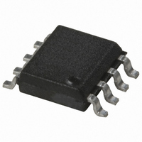
HCPL-0738-500 Avago Technologies US Inc., HCPL-0738-500 Datasheet - Page 6

HCPL-0738-500
Manufacturer Part Number
HCPL-0738-500
Description
OPTOCOUPLER 15MBD 2CH 8-SOIC
Manufacturer
Avago Technologies US Inc.
Datasheet
1.HCPL-0738-500.pdf
(8 pages)
Specifications of HCPL-0738-500
Package / Case
8-SOIC (0.154", 3.90mm Width)
Voltage - Isolation
3750Vrms
Number Of Channels
2, Unidirectional
Current - Output / Channel
2mA
Data Rate
15MBd
Propagation Delay High - Low @ If
35ns @ 12mA
Current - Dc Forward (if)
20mA
Input Type
DC
Output Type
Open Collector
Mounting Type
Surface Mount
Isolation Voltage
3750 Vrms
Maximum Continuous Output Current
2 mA
Maximum Fall Time
25 ns
Maximum Forward Diode Current
20 mA
Maximum Rise Time
20 ns
Minimum Forward Diode Voltage
1.3 V
Output Device
Logic Gate Photo IC
Configuration
2 Channel
Maximum Baud Rate
15 MBps
Maximum Forward Diode Voltage
1.8 V
Maximum Operating Temperature
+ 100 C
Minimum Operating Temperature
- 40 C
Lead Free Status / RoHS Status
Contains lead / RoHS non-compliant
Available stocks
Company
Part Number
Manufacturer
Quantity
Price
Company:
Part Number:
HCPL-0738-500E
Manufacturer:
AVAGO
Quantity:
300
Package Characteristics
All typicals at T
Parameter
Input-Output Insulation
Input-Output Momentary
Withstand Voltage
Input-Output Resistance
Input-Output Capacitance
Notes:
1. t
2. PWD is defined as |t
3. t
4. CM
5. CM
Figure 1. Typical input diode forward characteristic.
Figure 4. Typical logic low O/P supply current vs.
temperature.
6
signal. t
V
the recommended operating conditions.
0.001
11.6
11.4
11.2
11.0
10.8
10.6
10.4
10.2
10.0
PSK
1000
PHL
0.01
O
9.8
9.6
100
1.0
0.1
10
signal.
H
L
-40
is equal to the magnitude of the worst case difference in t
propagation delay is measured from the 50% level on the rising edge of the input pulse to the 2.5 V level of the falling edge of the V
1.1
is the maximum tolerable rate of fall of the common mode voltage to assure that the output will remain in a low logic state.
is the maximum tolerable rate of rise of the common mode voltage to assure that the output will remain in a high logic state.
V
PLH
V
DD
-20
F
T
1.2
A
– FORWARD VOLTAGE – V
= 5.0 V
A
propagation delay is measured from the 50% level on the falling edge of the input pulse to the 2.5 V level of the rising edge of the
= 5˚C.
V
+
–
– TEMPERATURE – °C
F
0
I
F
1.3
20
PHL
- t
40
1.4
PLH
|.
T
60
A
= 25°C
1.5
Symbol
I
V
R
C
I-O
I
80
I-O
ddl
ISO
I-O
100
1.6
Figure 5. Typical switching speed vs. pulse input cur-
rent.
Figure 2. Typical input threshold current vs. tempera-
ture.
50
45
40
35
30
25
20
15
10
Min.
3750
8
7
6
5
4
3
2
1
0
5
0
-40
PWD CH 1
T
5
I
V
T
V
I
F
phl
OL
DD
A
DD
-20
– PULSE INPUT CURRENT – mA
= 25 °C
6
CH 1
= 20 µA
T
= 5.0 V
= 5.0 V
PHL
A
7
– TEMPERATURE – °C
0
HCPL-0738 fig 5
and/or t
Typ.
10
0.6
8
T
1
20
plh
9
CH 1
10
PLH
40
T
11
that will be seen between units at any given temperature within
phl
60
T
PWD CH 2
12 13
Max.
1
plh
CH 2
I
I
CH 2
80
th
th
1
2
14
100
Units
µA
V rms
Ω
pF
Figure 3. Typical logic high O/P supply current vs.
temperature.
10.0
9.5
9.0
8.5
8.0
7.5
7.0
6.5
6.0
-40
Test Conditions
5% RH, t = 5 s
V
T
RH ≤ 50%, t = 1 min.,
T
V
f = 1 MHz, T
V
A
A
I-O
I-O
= 5˚C
= 5˚C
DD
-20
= 3 kV DC,
= 500 V DC
T
= 5.0 V
A
– TEMPERATURE – °C
0
A
= 5˚C
20
40
60
I
80
ddh
O
100


