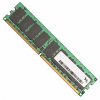
MT16HTF12864AY-53ED1 Micron Technology Inc, MT16HTF12864AY-53ED1 Datasheet

MT16HTF12864AY-53ED1
Specifications of MT16HTF12864AY-53ED1
Related parts for MT16HTF12864AY-53ED1
MT16HTF12864AY-53ED1 Summary of contents
Page 1
DDR2 SDRAM Unbuffered DIMM MT16HTF6464A – 512MB MT16HTF12864A – 1GB MT16HTF25664A – 2GB For component specifications, refer to the Micron’s Web site: Features • 240-pin, unbuffered, dual in-line memory module (UDIMM) • Fast data transfer rates: PC2-3200, PC2-4200, PC2- 5300, ...
Page 2
... MT16HTF25664AY-53E__ MT16HTF25664AY-40E__ 2GB Notes: 1. All part numbers end with a two-place code (not shown), designating component and PCB revisions. Consult factory for current revision codes. Example: MT16HTF12864AY-80ED4. PDF: 09005aef80f09084/Source: 09005aef80f09068 HTF16C64_128_256x64AG.fm - Rev. D 5/06 EN 512MB, 1GB, 2GB: (x64, DR) 240-Pin DDR2 SDRAM UDIMM 512MB 8K 8K (A0– ...
Page 3
Pin Assignments and Descriptions Table 4: Pin Assignment 240-pin DIMM Front Pin Symbol Pin Symbol Pin DQ19 61 REF DQ0 33 DQ24 63 4 DQ1 34 DQ25 64 5 ...
Page 4
Table 5: Pin Descriptions Pin numbers may not correlate with symbols; refer to Table 4 on page 3 for more information Pin Numbers 77, 195 ODT0, ODT1 137, 138, 185, 186, 220, 221 CK0, CK0#, CK1, CK1#, CK2, CK2# 52, ...
Page 5
Table 5: Pin Descriptions Pin numbers may not correlate with symbols; refer to Table 4 on page 3 for more information Pin Numbers 120 101, 239, 240 10, 12, 13, 21, 22, 24, DQ0–DQ63 25, 30, 31, ...
Page 6
... Functional Block Diagram Unless otherwise noted, resistor values are 22Ω. Micron module part numbers are explained in the module part numbering guide at Modules use the following DDR2 SDRAM devices: MT47H32M8BT (512MB); MT47H64M8BT (1GB); and MT47H128M8BT (2GB). Figure 3: Functional Block Diagram S1# S0# 25pF ...
Page 7
... READs and by the memory controller during WRITEs. DQS is edge-aligned with data for READs and center-aligned with data for WRITEs. DDR2 modules operate from a differential clock (CK and CK#); the crossing of CK going HIGH and CK# going LOW will be referred to as the positive edge of CK. Commands (address and control signals) are registered at every positive edge of CK ...
Page 8
... Simulations can then render a considerably more accurate result. JEDEC modules are now designed by using simula- tions to close timing budgets. PDF: 09005aef80f09084/Source: 09005aef80f09068 HTF16C64_128_256x64AG ...
Page 9
Table 7: DDR2 I Specifications and Conditions – 512MB DD Values shown for DDR2 SDRAM components only Parameter/Condition Operating one device bank active-precharge current RAS = RAS MIN ( ...
Page 10
Table 8: DDR2 I Specifications and Conditions – 1GB DD Values shown for DDR2 SDRAM components only Parameter/Condition Operating one device bank active-precharge current RAS = RAS MIN ( ...
Page 11
Table 9: DDR2 I Specifications and Conditions – 2GB DD Values shown for DDR2 SDRAM components only Parameter/Condition Operating one device bank active-precharge current RAS = RAS MIN ( ...
Page 12
AC Timing and Operating Conditions Recommended AC operating conditions are given in the DDR2 component data sheets. Component specifications are available on Micron’s Web site: Module speed grades correlate with component speed grades as shown in the following table: Table ...
Page 13
Serial Presence-Detect SPD Clock and Data Conventions Data states on the SDA line can change only during SCL LOW. SDA state changes during SCL HIGH are reserved for indicating start and stop conditions (Figures 4 and 5 on page 14). ...
Page 14
Figure 4: Data Validity SCL SDA Figure 5: Definition of Start and Stop SCL SDA Figure 6: Acknowledge Response From Receiver SCL from master Data output from transmitter Data output from receiver PDF: 09005aef80f09084/Source: 09005aef80f09068 HTF16C64_128_256x64AG.fm - Rev. D 5/06 ...
Page 15
Table 11: EEPROM Device Select Code The most significant bit (b7) is sent first Select Code Memory area select code (two arrays) Protection register select code Table 12: EEPROM Operating Modes Mode Current address READ Random address READ Sequential READ ...
Page 16
Table 13: Serial Presence-Detect EEPROM DC Operating Conditions All voltages referenced to V Parameter/Condition Supply voltage Input high voltage: Logic 1; All inputs Input low voltage: Logic 0; All inputs Output low voltage 3mA OUT Input leakage current: ...
Page 17
Table 15: Serial Presence-Detect Matrix “1”/“0”: Serial Data, “driven to HIGH”/“driven to LOW”; table notes located on page 19 Byte Description 0 Number of SPD bytes used by Micron 1 Total number of bytes in SPD device 2 Fundamental memory ...
Page 18
Table 15: Serial Presence-Detect Matrix “1”/“0”: Serial Data, “driven to HIGH”/“driven to LOW”; table notes located on page 19 Byte Description 28 MIN row active to row active, 29 MIN RAS#-to-CAS# delay MIN RAS# pulse width, RAS 31 ...
Page 19
Table 15: Serial Presence-Detect Matrix “1”/“0”: Serial Data, “driven to HIGH”/“driven to LOW”; table notes located on page 19 Byte Description 64 Manufacturer’s JEDEC ID code 65-71 Manufacturer’s JEDEC ID code 72 Manufacturing location 73-90 Module part number (ASCII) 91 ...
Page 20
Module Dimensions Figure 8: 240-pin DIMM DDR2 Module Dimensions 2.00 (0.079) R (4X 2.50 (0.098) D (2X) 2.30 (0.091) TYP. PIN 1 1.0 (0.039) TYP. U11 U12 PIN 240 55.0 (2.165) TYP. Notes: 1. All dimensions are in ...
Page 21
Revision History Rev. D, Released (No Mark ...


