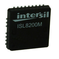
ISL8200MIRZ Intersil, ISL8200MIRZ Datasheet - Page 20

ISL8200MIRZ
Manufacturer Part Number
ISL8200MIRZ
Description
IC BUCK SYNC ADJ 10A 23-QFN
Manufacturer
Intersil
Type
Point of Load (POL) Non-Isolatedr
Datasheet
1.ISL8200MIRZ.pdf
(23 pages)
Specifications of ISL8200MIRZ
Output
0.6 ~ 6V
Number Of Outputs
1
Power (watts)
60W
Mounting Type
Surface Mount
Voltage - Input
3 ~ 20V
Package / Case
23-QFN
1st Output
0.6 ~ 6 VDC @ 10A
Size / Dimension
0.59" L x 0.59" W x 0.09" H (15mm x 15mm x 2.2mm)
Power (watts) - Rated
60W
Operating Temperature
-40°C ~ 85°C
Current - Output
10A
Voltage - Output
0.6 ~ 6 V
Frequency - Switching
700kHz ~ 1.5MHz
Synchronous Rectifier
Yes
Rohs Compliant
Yes
Lead Free Status / RoHS Status
Lead free / RoHS Compliant
3rd Output
-
2nd Output
-
Available stocks
Company
Part Number
Manufacturer
Quantity
Price
Part Number:
ISL8200MIRZ
Manufacturer:
INTERSIL
Quantity:
20 000
Thermal Vias
A grid of 1.0mm to 1.2mm pitch thermal vias, which
drops down and connects to buried copper plane(s),
should be placed under the thermal land. The vias should
be about 0.3mm to 0.33mm in diameter with the barrel
plated to about 1.0 ounce copper. Although adding more
vias (by decreasing via pitch) will improve the thermal
performance, diminishing returns will be seen as more
and more vias are added. Simply use as many vias as
practical for the thermal land size and your board design
rules allow.
Stencil Pattern Design
Reflowed solder joints on the perimeter I/O lands should
have about a 50µm to 75µm (2mil to 3mil) standoff
height. The solder paste stencil design is the first step in
developing optimized, reliable solder joins. Stencil
aperture size to land size ratio should typically be 1:1. The
aperture width may be reduced slightly to help prevent
solder bridging between adjacent I/O lands. To reduce
solder paste volume on the larger thermal lands, it is
recommended that an array of smaller apertures be used
instead of one large aperture. It is recommended that the
stencil printing area cover 50% to 80% of the PCB layout
pattern. A typical solder stencil pattern is shown in the
Package Outline Drawing L23.15x15 on page 22. The gap
width between pad to pad is 0.6mm. The user should
consider the symmetry of the whole stencil pattern when
designing its pads. A laser cut, stainless steel stencil with
electropolished trapezoidal walls is recommended.
Electropolishing “smooths” the aperture walls resulting in
reduced surface friction and better paste release which
reduces voids. Using a trapezoidal section aperture (TSA)
also promotes paste release and forms a "brick like" paste
deposit that assists in firm component placement. A
0.1mm to 0.15mm stencil thickness is recommended for
this large pitch (1.3mm) QFN.
20
ISL8200M
Reflow Parameters
Due to the low mount height of the QFN, "No Clean" Type 3
solder paste per ANSI/J-STD-00 is recommended. Nitrogen
purge is also recommended during reflow. A system board
reflow profile depends on the thermal mass of the entire
populated board, so it is not practical to define a specific
soldering profile just for the QFN. The profile given in
Figure 33 is provided as a guideline, to be customized for
varying manufacturing practices and applications.
300
250
200
150
100
50
0
0
SLOW RAMP AND
SOAK FROM +100°C TO
+180°C FOR 90s~120s
FIGURE 33. TYPICAL REFLOW PROFILE
RAMP RATE ≤1.5°C FROM +70°C TO +90°C
100
PEAK TEMPERATURE +230°C~+245°C;
KEEP ABOUT 30s ABOVE +220°C
150
DURATION (s)
200
250
February 26, 2010
50
FN6727.1
300


