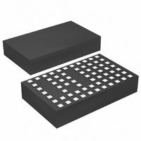
LTM4608EV#PBF Linear Technology, LTM4608EV#PBF Datasheet - Page 11

LTM4608EV#PBF
Manufacturer Part Number
LTM4608EV#PBF
Description
IC DC/DC UMODULE 8A 68-LGA
Manufacturer
Linear Technology
Series
µModuler
Type
Point of Load (POL) Non-Isolatedr
Datasheet
1.LTM4608IVPBF.pdf
(26 pages)
Specifications of LTM4608EV#PBF
Design Resources
LTM4608 Spice Model
Output
0.6 ~ 5 V
Number Of Outputs
1
Power (watts)
40W
Mounting Type
Surface Mount
Voltage - Input
2.7 ~ 5.5 V
Package / Case
68-LGA
1st Output
0.6 ~ 5 VDC @ 8A
Size / Dimension
0.59" L x 0.35" W x 0.11" H (15mm x 9mm x 2.8mm)
Power (watts) - Rated
40W
Operating Temperature
-40°C ~ 85°C
Efficiency
95%
Dc To Dc Converter Type
Step Down
Pin Count
68
Input Voltage
5.5V
Output Voltage
0.6 to 5V
Switching Freq
1.7MHz
Output Current
8A
Package Type
LGA
Output Type
Adjustable
Switching Regulator
Yes
Load Regulation
0.75%
Line Regulation
0.2%/V
Mounting
Surface Mount
Input Voltage (min)
2.375V
Operating Temperature Classification
Industrial
Lead Free Status / RoHS Status
Lead free / RoHS Compliant
3rd Output
-
2nd Output
-
Lead Free Status / Rohs Status
Compliant
Available stocks
Company
Part Number
Manufacturer
Quantity
Price
Without considering the inductor current ripple, the RMS
current of the input capacitor can be estimated as:
In the above equation, η% is the estimated efficiency of
the power module. The bulk capacitor can be a switcher-
rated electrolytic aluminum capacitor, polymer capacitor
for bulk input capacitance due to high inductance traces
or leads. If a low inductance plane is used to power the
device, then only one 10µF ceramic is required. The three
internal 10µF ceramics are typically rated for 2A of RMS
ripple current, so the ripple current at the worse case for
8A maximum current is 4A or less.
Output Capacitors
The LTM4608 is designed for low output voltage ripple
noise. The bulk output capacitors defined as C
chosen with low enough effective series resistance (ESR)
to meet the output voltage ripple and transient require-
ments. C
ESR polymer capacitor or ceramic capacitor. The typical
output capacitance range is from 47µF to 220µF . Additional
output filtering may be required by the system designer,
if further reduction of output ripple or dynamic transient
spikes is desired. Table 3 shows a matrix of different output
voltages and output capacitors to minimize the voltage
droop and overshoot during a 3A/µs transient. The table
optimizes total equivalent ESR and total bulk capacitance
to optimize the transient performance. Stability criteria are
considered in the Table 3 matrix, and the Linear Technology
LTpowerCAD™ Design Tool is available for stability analysis.
Multiphase operation will reduce effective output ripple as
a function of the number of phases. Application Note 77
discusses this noise reduction versus output ripple cur-
rent cancellation, but the output capacitance will be more
a function of stability and transient response. The Linear
Technology LTpowerCAD Design Tool will calculate the
output ripple reduction as the number phases implemented
increases by N times.
APPLICATIONS INFORMATION
I
CIN(RMS)
OUT
=
can be a low ESR tantalum capacitor, a low
I
OUT(MAX)
η%
• D • 1– D
(
)
OUT
are
Burst Mode Operation
The LTM4608 is capable of Burst Mode operation in which
the power MOSFETs operate intermittently based on load
demand, thus saving quiescent current. For applications
where maximizing the efficiency at very light loads is a
high priority, Burst Mode operation should be applied. To
enable Burst Mode operation, simply tie the MODE pin to
V
is set to approximately 20% of the maximum peak current
value in normal operation even though the voltage at the
I
drops when the inductor’s average current is greater than
the load requirement. As the I
the BURST comparator trips, causing the internal sleep
line to go high and turn off both power MOSFETs.
In sleep mode, the internal circuitry is partially turned off,
reducing the quiescent current to about 450µA. The load cur-
rent is now being supplied from the output capacitor. When
the output voltage drops, causing I
the internal sleep line goes low, and the LTM4608 resumes
normal operation. The next oscillator cycle will turn on the
top power MOSFET and the switching cycle repeats.
Pulse-Skipping Mode Operation
In applications where low output ripple and high efficiency
at intermediate currents are desired, pulse-skipping mode
should be used. Pulse-skipping operation allows the
LTM4608 to skip cycles at low output loads, thus increasing
efficiency by reducing switching loss. Floating the MODE
pin or tying it to V
This allows discontinuous conduction mode (DCM) opera-
tion down to near the limit defined by the chip’s minimum
on-time (about 100ns). Below this output current level,
the converter will begin to skip cycles in order to main-
tain output regulation. Increasing the output load current
slightly, above the minimum required for discontinuous
conduction mode, allows constant frequency PWM.
TH
IN
. During this operation, the peak current of the inductor
pin indicates a lower value. The voltage at the I
IN
/2 enables pulse-skipping operation.
TH
voltage drops below 0.2V,
TH
to rise above 0.25V,
LTM4608
11
TH
4608fc
pin


