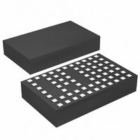
LTM4608EV#PBF Linear Technology, LTM4608EV#PBF Datasheet - Page 17

LTM4608EV#PBF
Manufacturer Part Number
LTM4608EV#PBF
Description
IC DC/DC UMODULE 8A 68-LGA
Manufacturer
Linear Technology
Series
µModuler
Type
Point of Load (POL) Non-Isolatedr
Datasheet
1.LTM4608IVPBF.pdf
(26 pages)
Specifications of LTM4608EV#PBF
Design Resources
LTM4608 Spice Model
Output
0.6 ~ 5 V
Number Of Outputs
1
Power (watts)
40W
Mounting Type
Surface Mount
Voltage - Input
2.7 ~ 5.5 V
Package / Case
68-LGA
1st Output
0.6 ~ 5 VDC @ 8A
Size / Dimension
0.59" L x 0.35" W x 0.11" H (15mm x 9mm x 2.8mm)
Power (watts) - Rated
40W
Operating Temperature
-40°C ~ 85°C
Efficiency
95%
Dc To Dc Converter Type
Step Down
Pin Count
68
Input Voltage
5.5V
Output Voltage
0.6 to 5V
Switching Freq
1.7MHz
Output Current
8A
Package Type
LGA
Output Type
Adjustable
Switching Regulator
Yes
Load Regulation
0.75%
Line Regulation
0.2%/V
Mounting
Surface Mount
Input Voltage (min)
2.375V
Operating Temperature Classification
Industrial
Lead Free Status / RoHS Status
Lead free / RoHS Compliant
3rd Output
-
2nd Output
-
Lead Free Status / Rohs Status
Compliant
Available stocks
Company
Part Number
Manufacturer
Quantity
Price
APPLICATIONS INFORMATION
Slope Compensation
The module has already been internally compensated for
all output voltages. Table 3 is provided for most application
requirements. A spice model will be provided for other
control loop optimization. For single module operation,
connect I
pins together and then connect to SGND at one point. Tie
I
Output Margining
For a convenient system stress test on the LTM4608’s
output, the user can program the LTM4608’s output to
±5%, ±10% or ±15% of its normal operational voltage.
The margin pin with a voltage divider is driven with a
small three-state gate as shown in Figure 18, for the three
margin states (high, low, no margin). When the MGN
pin is < 0.3V, it forces negative margining in which the
output voltage is below the regulation point. When MGN is
> V
lation point. The amount of output voltage margining is
TH
IN
pins together to share currents evenly for all phases.
– 0.3V, the output voltage is forced above the regu-
Figure 7. 3.3V
THM
4.0
3.5
3.0
2.5
2.0
1.5
1.0
0.5
0
0
pin to SGND. For parallel operation, tie I
IN
2
, 2.5V and 1.5V
LOAD CURRENT (A)
4
3.3V
3.3V
6
OUT
IN
IN
1.5V
2.5V
Power Loss
4608 F07
OUT
OUT
8
THM
determined by the BSEL pin. When BSEL is low, it is 5%.
When BSEL is high, it is 10%. When BSEL is floating,
it is 15%. When margining is active, the internal output
overvoltage and undervoltage comparators are disabled
and PGOOD remains high. Margining is disabled by tying
the MGN pin to a voltage divider as shown in Figure 20.
Thermal Considerations and Output Current Derating
The power loss curves in Figures 7 and 8 can be used
in coordination with the load current derating curves in
Figures 9 to 16 for calculating an approximate θ
module with various heat sinking methods. Thermal models
are derived from several temperature measurements at
the bench, and thermal modeling analysis. Thermal Ap-
plication Note 103 provides a detailed explanation of the
analysis for the thermal models and the derating curves.
Tables 4 and 5 provide a summary of the equivalent θ
for the noted conditions. These equivalent θ
are correlated to the measured values and improve with
air flow. The junction temperature is maintained at 125°C
or below for the derating curves.
Figure 8. 5V
4.0
3.5
3.0
2.5
2.0
1.5
1.0
0.5
0
0
IN
2
, 3.3V and 1.5V
LOAD CURRENT (A)
4
5V
5V
OUT
6
IN
IN
1.5V
3.3V
Power Loss
LTM4608
4608 F08
OUT
OUT
8
JA
parameters
JA
17
for the
4608fc
JA


