MA330012 Microchip Technology, MA330012 Datasheet - Page 291
MA330012
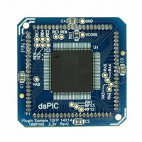
Manufacturer Part Number
MA330012
Description
MODULE DSPIC33 100P TO 84QFP
Manufacturer
Microchip Technology
Specifications of MA330012
Accessory Type
Plug-In Module (PIM) 80p - dsPIC33FJ256GP710
Kit Contents
DsPIC33 GP 100P To 80P TQFP Plug-In Module
Tool / Board Applications
General Purpose MCU, MPU, DSP, DSC
Silicon Manufacturer
Microchip
Core Architecture
DsPIC
Core Sub-architecture
DsPIC33
Silicon Core Number
DsPIC33F
Silicon Family Name
DsPIC33FJxxGPxxx
Rohs Compliant
Yes
For Use With
DsPICDEM 80-Pin Starter Board (DM300019)
Lead Free Status / RoHS Status
Lead free / RoHS Compliant
For Use With/related Products
dsPICDEM (DM300019)
Lead Free Status / RoHS Status
Lead free / RoHS Compliant, Lead free / RoHS Compliant


23.0
dsPIC33F devices include several features intended to
maximize application flexibility and reliability, and mini-
mize cost through elimination of external components.
These are:
• Flexible Configuration
• Watchdog Timer (WDT)
• Code Protection and CodeGuard™ Security
• JTAG Boundary Scan Interface
• In-Circuit Serial Programming™ (ICSP™)
• In-Circuit Emulation
23.1
The Configuration bits can be programmed (read as
‘0’), or left unprogrammed (read as ‘1’), to select vari-
ous device configurations. These bits are mapped
starting at program memory location 0xF80000.
TABLE 23-1:
© 2007 Microchip Technology Inc.
0xF80000 FBS
0xF80002 FSS
0xF8004
0xF8006
0xF8008
0xF800A
0xF800C
0xF800E
0xF8010
0xF8012
0xF8014
0xF8016
Note 1:
Address
Note:
2:
3:
4:
SPECIAL FEATURES
Configuration Bits
FGS
FOSCSEL
FOSC
FWDT
FPOR
RESERVED3
FUID0
FUID1
FUID2
FUID3
On the dsPIC33F General Purpose Family devices (dsPIC33FJXXXGPXXX), these bits are reserved (read as ‘1’ and
must be programmed as ‘1’).
These reserved bits read as ‘1’ and must be programmed as ‘1’.
Unimplemented bits are read as ‘0’.
This reserved bit is a read-only copy of the GCP bit.
This data sheet summarizes the features
of this group of dsPIC33F devices. It is not
intended to be a comprehensive reference
source. To complement the information in
this data sheet, refer to the “dsPIC30F
Family Reference Manual” (DS70046).
Name
DEVICE CONFIGURATION REGISTER MAP
PWMPIN
FWDTEN
IESO
Bit 7
—
FCKSM<1:0>
RBS<1:0>
RSS<1:0>
(1)
HPOL
WINDIS
Bit 6
—
—
(1)
Preliminary
LPOL
TEMP
Bit 5
—
—
—
—
—
(1)
The device Configuration register map is shown in
Table 23-1.
The individual Configuration bit descriptions for the
FBS, FSS, FGS, FOSCSEL, FOSC, FWDT, FPOR and
FICD Configuration registers are shown in Table 23-2.
Note that address 0xF80000 is beyond the user program
memory space. In fact, it belongs to the configuration
memory space (0x800000-0xFFFFFF) which can only be
accessed using table reads and table writes.
The upper byte of all device Configuration registers
should always be ‘1111
appear to be NOP instructions in the remote event that
their locations are ever executed by accident. Since
Configuration bits are not implemented in the
corresponding locations, writing ‘1’s to these locations
has no effect on device operation.
To prevent inadvertent configuration changes during
code execution, all programmable Configuration bits
are write-once. After a bit is initially programmed during
a power cycle, it cannot be written to again. Changing
a device configuration requires that power to the device
be cycled.
User Unit ID Byte 0
User Unit ID Byte 1
User Unit ID Byte 2
User Unit ID Byte 3
WDTPRE
Bit 4
Reserved
—
—
—
—
—
—
(2)
Bit 3
—
—
—
BSS<2:0>
SSS<2:0>
OSCIOFNC
WDTPOST<3:0>
GSS1
Bit 2
1111’. This makes them
dsPIC33F
FPWRT<2:0>
DS70165E-page 289
GSS0
POSCMD<1:0>
Bit 1
GWRP
BWRP
SWRP
Bit 0
Related parts for MA330012
Image
Part Number
Description
Manufacturer
Datasheet
Request
R

Part Number:
Description:
Manufacturer:
Microchip Technology Inc.
Datasheet:
Part Number:
Description:
Manufacturer:
Microchip Technology Inc.
Datasheet:
Part Number:
Description:
Manufacturer:
Microchip Technology Inc.
Datasheet:
Part Number:
Description:
Manufacturer:
Microchip Technology Inc.
Datasheet:
Part Number:
Description:
Manufacturer:
Microchip Technology Inc.
Datasheet:
Part Number:
Description:
Manufacturer:
Microchip Technology Inc.
Datasheet:
Part Number:
Description:
Manufacturer:
Microchip Technology Inc.
Datasheet:
Part Number:
Description:
Manufacturer:
Microchip Technology Inc.
Datasheet: