MA330012 Microchip Technology, MA330012 Datasheet - Page 80
MA330012
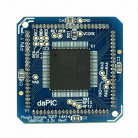
Manufacturer Part Number
MA330012
Description
MODULE DSPIC33 100P TO 84QFP
Manufacturer
Microchip Technology
Specifications of MA330012
Accessory Type
Plug-In Module (PIM) 80p - dsPIC33FJ256GP710
Kit Contents
DsPIC33 GP 100P To 80P TQFP Plug-In Module
Tool / Board Applications
General Purpose MCU, MPU, DSP, DSC
Silicon Manufacturer
Microchip
Core Architecture
DsPIC
Core Sub-architecture
DsPIC33
Silicon Core Number
DsPIC33F
Silicon Family Name
DsPIC33FJxxGPxxx
Rohs Compliant
Yes
For Use With
DsPICDEM 80-Pin Starter Board (DM300019)
Lead Free Status / RoHS Status
Lead free / RoHS Compliant
For Use With/related Products
dsPICDEM (DM300019)
Lead Free Status / RoHS Status
Lead free / RoHS Compliant, Lead free / RoHS Compliant


dsPIC33F
4.2
The dsPIC33F Flash program memory array is
organized into rows of 64 instructions or 192 bytes.
RTSP allows the user to erase a page of memory,
which consists of eight rows (512 instructions) at a
time, and to program one row or one word at a time.
Table 26-11, DC Characteristics: Program Memory
shows typical erase and programming times. The 8-
row erase pages and single row write rows are edge-
aligned, from the beginning of program memory, on
boundaries of 1536 bytes and 192 bytes, respectively.
The program memory implements holding buffers that
can contain 64 instructions of programming data. Prior
to the actual programming operation, the write data
must be loaded into the buffers in sequential order. The
instruction words loaded must always be from a group
of 64 boundary.
The basic sequence for RTSP programming is to set up
a Table Pointer, then do a series of TBLWT instructions
to load the buffers. Programming is performed by set-
ting the control bits in the NVMCON register. A total of
64 TBLWTL and TBLWTH instructions are required to
load the instructions.
All of the table write operations are single-word writes
(two instruction cycles) because only the buffers are
written.
programming each row.
DS70165E-page 78
RTSP Operation
A
programming
cycle
is
required
Preliminary
for
4.3
There are two SFRs used to read and write the
program Flash memory: NVMCON and NVMKEY.
The NVMCON register (Register 4-1) controls which
blocks are to be erased, which memory type is to be
programmed and the start of the programming cycle.
NVMKEY is a write-only register that is used for write
protection. To start a programming or erase sequence,
the user must consecutively write 55h and AAh to the
NVMKEY register. Refer to Section 4.4 “Programming
Operations” for further details.
4.4
A complete programming sequence is necessary for
programming or erasing the internal Flash in RTSP
mode. A programming operation is nominally 4 ms in
duration and the processor stalls (waits) until the oper-
ation is finished. Setting the WR bit (NVMCON<15>)
starts the operation, and the WR bit is automatically
cleared when the operation is finished.
Control Registers
Programming Operations
© 2007 Microchip Technology Inc.
Related parts for MA330012
Image
Part Number
Description
Manufacturer
Datasheet
Request
R

Part Number:
Description:
Manufacturer:
Microchip Technology Inc.
Datasheet:
Part Number:
Description:
Manufacturer:
Microchip Technology Inc.
Datasheet:
Part Number:
Description:
Manufacturer:
Microchip Technology Inc.
Datasheet:
Part Number:
Description:
Manufacturer:
Microchip Technology Inc.
Datasheet:
Part Number:
Description:
Manufacturer:
Microchip Technology Inc.
Datasheet:
Part Number:
Description:
Manufacturer:
Microchip Technology Inc.
Datasheet:
Part Number:
Description:
Manufacturer:
Microchip Technology Inc.
Datasheet:
Part Number:
Description:
Manufacturer:
Microchip Technology Inc.
Datasheet: