DLP-FPGA-M DLP Design Inc, DLP-FPGA-M Datasheet - Page 2
DLP-FPGA-M
Manufacturer Part Number
DLP-FPGA-M
Description
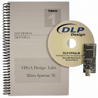
MODULE USB-TO-FPGA TOOL W/MANUAL
Manufacturer
DLP Design Inc
Datasheet
1.DLP-FPGA.pdf
(10 pages)
Specifications of DLP-FPGA-M
Main Purpose
Interface, USB to FPGA
Embedded
Yes, FPGA / CPLD
Utilized Ic / Part
FT2232D, XC3S250E-4TQ144
Primary Attributes
USB to FPGA, 40 I/O Pins, SRAM: 128k x 8
Secondary Attributes
4 Labs in Manual, 250k System Gates, 5.5k Logic Cells
Interface Type
USB, SPI
Product
Interface Modules
For Use With/related Products
XC3S250E-4TQ144
Lead Free Status / RoHS Status
Lead free / RoHS Compliant
Lead Free Status / RoHS Status
Lead free / RoHS Compliant, Lead free / RoHS Compliant
Other names
813-1009


1.0 INTRODUCTION
The DLP-FPGA Module is a low-cost, compact prototyping module that can be used for rapid proof of
concept or for educational environments. The module is based on the Xilinx Spartan 3E and Future
Technology Devices International’s FT2232D Dual-Channel USB IC. Used by itself or with the
optional 200-page training manual, the DLP-FPGA provides both the beginner as well as the
experienced engineer with a rapid path to developing FPGA-based designs. When combined with the
free WebPACK™ Tools from Xilinx, this module is more than sufficient for creating anything from
basic logical functions to a highly complex system controller.
As a bonus feature, one channel of the dual-channel USB interface is used to load user bit files
directly to the SPI Flash—no external programmer is required. This represents a savings of as much
as $200 in that no additional programming cable is required for configuring the FPGA. All that is
needed to load bit files to the DLP-FPGA is a Windows software utility (free with purchase), a
Windows PC and a USB cable. The module can also be programmed from within the Xilinx ISE tool
environment using a Xilinx programming cable (purchased separately).
The DLP-FPGA is fully compatible with the free ISE™ WebPACK™ tools from Xilinx. ISE WebPACK
offers the ideal development environment for FPGA designs with HDL synthesis and simulation,
implementation, device fitting and JTAG programming.
The DLP-FPGA has on-board voltage regulators that generate all required power supply voltages
from a single 5-volt source. Power for the module can be taken from either the host USB port or from
a user-supplied, external 5-volt power supply.
Connection to user electronics is made via a 50-pin, 0.9-inch wide, industry-standard 0.025 square
inch post DIP header. Other on-board features include a 128K x 8 static RAM IC for user projects,
and both JTAG and SPI Flash interface ports for connection to Xilinx programming tools.
2.0 TRAINING MANUAL
A 200+ page training manual for the DLP-FPGA is also available. While this manual is designed to
provide entry-level instruction for those new to designing with FPGAs, it is recommended for
developers who have some experience with FPGA products and associated development tools. An
ISE™ WebPACK™ Software installation DVD is included with the manual.
The manual is comprised of 5 Chapters and 4 Labs as outlined below:
Chapter 1: Installing the Xilinx ISE WebPACK tools and Understanding the Design Flow
Chapter 2: Lab 1: Implementing a Simple AND Gate: Create a New Project, Implement the Design,
View the Synthesized Design, View the Placed and Routed Design
Chapter 3: Lab 2: Heartbeat: Understanding the Digital Clock Manager (DCM), Methods of Starting
ISE Project Navigator, VHDL Module Structure, Utilizing Hierarchy, Adding the DCM Component,
Adding the Heartbeat Component, Connecting the Components, Synthesizing the Design Using XST,
Simulating the Design Using the ISE Simulator, Adding the User Constraint File, Implementing the
Design, Download the Design to the FPGA
Rev. 1.4 (November 2010)
2
© DLP Design, Inc.
Related parts for DLP-FPGA-M
Image
Part Number
Description
Manufacturer
Datasheet
Request
R

Part Number:
Description:
MODULE USB-TO-TTL PARL FIFO CONV
Manufacturer:
DLP Design Inc
Datasheet:

Part Number:
Description:
KIT DEV DLP LIGHTCOMANDER
Manufacturer:
Logic
Datasheet:

Part Number:
Description:
MODULE DATA-ACQUISITION 8-CH
Manufacturer:
DLP Design Inc
Datasheet:

Part Number:
Description:
MODULE DATA-ACQUISITION 20-CH
Manufacturer:
DLP Design Inc
Datasheet:

Part Number:
Description:
RFID READER/WRITER SNGL-CH OEM
Manufacturer:
DLP Design Inc
Datasheet:

Part Number:
Description:
Interface Modules & Development Tools DLP-245PL PACKAGED w/CCS Compiler
Manufacturer:
DLP Design Inc

Part Number:
Description:
Interface Modules & Development Tools DLP-245PB-G BOARD + CCS Compiler
Manufacturer:
DLP Design Inc
Datasheet:

Part Number:
Description:
Interface Modules & Development Tools DLP-TILT SENSOR ACCEL VIBRATION
Manufacturer:
DLP Design Inc

Part Number:
Description:
MODULE USB-MCU FT245RL W/16F877A
Manufacturer:
DLP Design Inc
Datasheet:

Part Number:
Description:
MODULE USB-TO-FPGA TRAINING TOOL
Manufacturer:
DLP Design Inc
Datasheet:

Part Number:
Description:
MODULE USB-MCU FT232R W/18F2410
Manufacturer:
DLP Design Inc
Datasheet:

Part Number:
Description:
MODULE USB-MCU FT245RL W/SX48
Manufacturer:
DLP Design Inc
Datasheet:

Part Number:
Description:
MODULE USB-MCU FT2232D W/16F877A
Manufacturer:
DLP Design Inc
Datasheet:

Part Number:
Description:
MODULE USB-TO-FPGA SPARTAN3
Manufacturer:
DLP Design Inc
Datasheet:

Part Number:
Description:
MOD USB-MCU FT245RL W/18LF8722
Manufacturer:
DLP Design Inc
Datasheet: