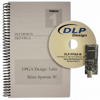
DLP-FPGA-M DLP Design Inc, DLP-FPGA-M Datasheet - Page 5

DLP-FPGA-M
Manufacturer Part Number
DLP-FPGA-M
Description
MODULE USB-TO-FPGA TOOL W/MANUAL
Manufacturer
DLP Design Inc
Datasheet
1.DLP-FPGA.pdf
(10 pages)
Specifications of DLP-FPGA-M
Main Purpose
Interface, USB to FPGA
Embedded
Yes, FPGA / CPLD
Utilized Ic / Part
FT2232D, XC3S250E-4TQ144
Primary Attributes
USB to FPGA, 40 I/O Pins, SRAM: 128k x 8
Secondary Attributes
4 Labs in Manual, 250k System Gates, 5.5k Logic Cells
Interface Type
USB, SPI
Product
Interface Modules
For Use With/related Products
XC3S250E-4TQ144
Lead Free Status / RoHS Status
Lead free / RoHS Compliant
Lead Free Status / RoHS Status
Lead free / RoHS Compliant, Lead free / RoHS Compliant
Other names
813-1009
8.0 USB DRIVERS
USB drivers for the following operating systems are available for download from the DLP Design
website at http://www.dlpdesign.com:
Notes:
9.0 USING THE DLP-FPGA
Select a power source via Header Pins 23 and 24, and connect the DLP-FPGA to the PC to initiate
the loading of USB drivers. The easiest way to do this is to connect Pins 23 and 24 to each other.
This will result in operational power being taken from the host PC. Once the drivers are loaded, the
DLP-FPGA is ready for use.
Rev. 1.4 (November 2010)
1. The bit file load utility only runs on the Windows platforms.
2. The bit file load utility requires the use of USB channel A, and channel A is dedicated to this
3. If you are using the dual-mode drivers from FTDI (CDM2.02.04) and wish to use the Virtual
COM Port (VCP) drivers for Channel B communications, then it may be necessary to disable
the D2XX drivers first via Device Manager. To do so, right click on the Channel B entry under
USB Controllers that appears when the DLP-FPGA is connected, select Properties, select the
Advanced tab, check the option for “Load VCP” and click OK. Once you unplug and then
replug the DLP-FPGA, a COM port should appear in Device Manager under Ports (COM &
LPT).
function.
W
W
i
i
W
W
n
W
n
W
W
W
d
d
i
i
i
i
n
n
o
n
o
n
i
i
n
d
n
d
w
w
d
d
d
d
o
o
o
o
s
s
Top View (Interface Headers on bottom of PCB)
Pin 25
o
o
w
w
w
w
Pin 1
S
S
w
w
s
s
s
s
e
e
s
s
X
X
r
9
r
9
v
v
2
2
8
P
8
P
e
e
0
0
,
,
r
x
r
0
x
0
M
M
6
6
2
0
2
0
E
E
4
4
0
0
0
0
3
3
SRAM
FPGA
5
M
M
M
M
M
M
a
L
a
a
a
L
a
a
Pin 26
Pin 50
c
c
c
c
i
c
c
i
n
n
O
O
O
O
O
O
u
u
x
S
x
S
S
S
S
S
X
X
9
9
8
8
© DLP Design, Inc.


