KDC2710CEVAL Intersil, KDC2710CEVAL Datasheet - Page 6
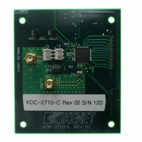
KDC2710CEVAL
Manufacturer Part Number
KDC2710CEVAL
Description
DAUGHTER CARD FOR KAD2710
Manufacturer
Intersil
Series
FemtoCharge™r
Datasheets
1.KAD2710C-10Q68.pdf
(16 pages)
2.KMB-001LEVALZ.pdf
(7 pages)
3.KDC5514EVALZ.pdf
(9 pages)
Specifications of KDC2710CEVAL
Number Of Adc's
1
Number Of Bits
10
Sampling Rate (per Second)
275M
Data Interface
Parallel
Inputs Per Adc
1 Differential
Input Range
1.5 Vpp
Power (typ) @ Conditions
261mW @ 275MSPS
Voltage Supply Source
Single Supply
Operating Temperature
-40°C ~ 85°C
Utilized Ic / Part
KAD2710C-27, KMB001 Motherboard
For Use With
KMB001LEVAL - MOTHERBOARD FOR LVDS ADC CARD
Lead Free Status / RoHS Status
Lead free / RoHS Compliant


The MATLAB component runtime installation is now complete.
Running the Intersil Konverter Analyzer
Software
To run the Intersil Konverter Analyzer software:
Specifications Definitions
Analog Input Bandwidth is the analog input frequency at which
the spectral output power at the fundamental frequency (as
determined by FFT analysis) is reduced by 3dB from its
low-frequency value. This is also referred to as Full Power
Bandwidth.
Aperture Delay or Sampling Delay is the time required after the
rise of the clock input for the sampling switch to open, at which
time the signal is held for conversion.
Aperture Jitter is the RMS variation in aperture delay for a set of
samples.
Clock Duty Cycle is the ratio of the time the clock wave is at logic
high to the total time of one clock period.
Differential Non-Linearity (DNL) is the deviation of any code width
from an ideal 1 LSB step.
Effective Number of Bits (ENOB) is an alternate method of
specifying Signal to Noise-and-Distortion Ratio (SINAD). In dB, it is
calculated as: ENOB = (SINAD - 1.76)/6.02
Integral Non-Linearity (INL) is the deviation of each individual
code from a line drawn from zero (1/2 LSB below the first code
transition) through positive full-scale (1/2 LSB above the last
9. In the InstallShield Wizard Completed window, click Finish.
1. On the desktop, double-click the Intersil Konverter Analyzer
2. If the Welcome to the Found New Hardware Wizard window
3. If the Hardware Installation window opens, click Continue
Runtime X.X Installer Information window, click OK. The
InstallShield Wizard Completed window appears.
shortcut icon. The application uncompresses the first time it
runs; subsequently, it starts immediately.
opens, click the No, not this time radio button and then click
Next.
Anyway.
6
Application Note 1434
code transition). The deviation of any given code from this line is
measured from the center of that code.
Least Significant Bit (LSB) is the bit that has the smallest value or
weight in a digital word. Its value in terms of input voltage is
V
Missing Codes are output codes that are skipped and will never
appear at the ADC output. These codes cannot be reached with
any input value.
Most Significant Bit (MSB) is the bit that has the largest value or
weight. Its value in terms of input voltage is V
Pipeline Delay is the number of clock cycles between the
initiation of a conversion and the appearance of the data at the
output pins.
Power Supply Rejection Ratio (PSRR) is the ratio of a change in
input offset voltage to a change in power supply voltage.
Signal to Noise-and-Distortion (SINAD) is the ratio of the RMS
signal amplitude to the RMS value of the sum of all other
spectral components below one-half the clock frequency,
including harmonics but excluding DC.
Signal-to-Noise Ratio (without Harmonics) is the ratio of the RMS
signal amplitude to the sum of all other spectral components
below one-half the sampling frequency, excluding harmonics and
DC.
Spurious-Free-Dynamic Range (SFDR) is the ratio of the RMS
signal amplitude to the RMS value of the peak spurious spectral
component. The peak spurious spectral component may or may
not be a harmonic.
Appendix A
Source Requirements
Source jitter and noise will degrade performance. For best test
results, a combined jitter (for both clock and signal sources) that
does not exceed 200fs is recommended.
Sample Clock and Input Signal Source Setup
Sample clock settings:
• 50MHz to 500MHz sine, +10dBm
Signal settings:
• 0.4MHz to 250MHz, +7dBm to +10dBm (depending on analog
FS
input attenuation)
/2
N-1
where N is the resolution in bits.
FS
/2.
March 31, 2011
AN1434.4
Related parts for KDC2710CEVAL
Image
Part Number
Description
Manufacturer
Datasheet
Request
R

Part Number:
Description:
Intersil Corporation [CMOS Serial Controller Interface]
Manufacturer:
Intersil Corporation
Datasheet:
Part Number:
Description:
Manufacturer:
Intersil Corporation
Datasheet:
Part Number:
Description:
357-036-542-201 CARDEDGE 36POS DL .156 BLK LOPRO
Manufacturer:
Intersil Corporation
Datasheet:
Part Number:
Description:
1024-Word x 4-Bit LSI Static RAM
Manufacturer:
Intersil Corporation
Datasheet:
Part Number:
Description:
General Purpose NPN Transistor Arrays FN341.4
Manufacturer:
Intersil Corporation
Datasheet:
Part Number:
Description:
CMOS 16-Bit Microprocessor
Manufacturer:
Intersil Corporation
Datasheet:
Part Number:
Description:
Manufacturer:
Intersil Corporation
Datasheet:
Part Number:
Description:
Manufacturer:
Intersil Corporation
Datasheet:
Part Number:
Description:
Manufacturer:
Intersil Corporation
Datasheet:
Part Number:
Description:
Manufacturer:
Intersil Corporation
Datasheet:
Part Number:
Description:
CMOS 6-Bit Latch and Decoder Memory Interfaces
Manufacturer:
Intersil Corporation
Datasheet:
Part Number:
Description:
CA3046General Purpose NPN Transistor Arrays
Manufacturer:
Intersil Corporation
Datasheet:
Part Number:
Description:
Manufacturer:
Intersil Corporation
Datasheet:
Part Number:
Description:
TR909 DLC/FLC SLIC with Low Power Standby
Manufacturer:
Intersil Corporation
Datasheet:
Part Number:
Description:
Manufacturer:
Intersil Corporation
Datasheet: