RDK-201 Power Integrations, RDK-201 Datasheet - Page 7
RDK-201
Manufacturer Part Number
RDK-201
Description
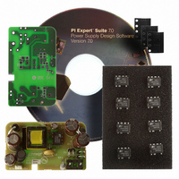
KIT REF DESIGN LINKSWITCH-CV
Manufacturer
Power Integrations
Series
LinkSwitch®-CVr
Type
MOSFET & Power Driverr
Specifications of RDK-201
Main Purpose
AC/DC, Primary Side
Outputs And Type
1, Isolated
Power - Output
6W
Voltage - Output
5V
Current - Output
1.2A
Voltage - Input
90 ~ 265VAC
Regulator Topology
Flyback
Board Type
Fully Populated
Utilized Ic / Part
LNK626
Product
Power Management Modules
Lead Free Status / RoHS Status
Lead free / RoHS Compliant
Frequency - Switching
-
Lead Free Status / Rohs Status
Lead free / RoHS Compliant
For Use With/related Products
LNK62x
Other names
596-1266


11-Nov-08
RDR-201 6 W LinkSwitch-CV Adapter
The clamp circuit formed by resistors R1 and R2 along with blocking diode D5 and
capacitor C3 ensures that the drain node voltage is well below the 700 V rating of the
internal MOSFET of U1. The clamp circuit is also carefully designed to reduce and
dampen any oscillation present in the voltage spike caused by the transformer’s leakage
inductance.
4.4 Output Rectification
The secondary output is rectified by diode D7 which is placed in the return leg to help
reduce EMI and simplify the transformer construction. An RC snubber circuit composed
of resistor R7 and capacitor C6 is placed across the output diode to also reduce high
frequency EMI. A stable output voltage is maintained by capacitor C7.
Inductor L2 and capacitor C8 form an LC post filter which helps to attenuate switching
noise and reduces output ripple. Resistor R8 is a preload resistor whose value has been
empirically chosen to provide the best possible regulation at light loads without
significantly affecting no-load input power or efficiency.
4.5 Feedback Winding
LinkSwitch-CV eliminates the need for an optocoupler for tight output voltage regulation,
as good as ±5 %, through the use of a feedback winding. The feedback (FB) pin voltage,
which is derived from the voltage divider formed by resistors R3 and R4, is sampled
approximately 2.5 µs after U1’s internal MOSFET turns off. Based upon this information
the device regulates the output voltage.
The feedback winding was also designed with more turns than necessary so that it may
act as a bias winding. The winding provides bias current to U1 through the bypass pin
(BP) and reduces the input power consumption during light loads and no-load conditions.
Resistor R6 helps to dampen out any ringing present on the feedback winding and
ensures that the waveform at the FB pin at 2.5 us is free from any ringing. Capacitor C5
provides a stable bias voltage while resistor R5 is chosen to supply the necessary BP pin
current. Capacitor C4 is the BP pin capacitor and should be placed as close as possible
to the BP pin and source pins of the device.
Power Integrations
Tel: +1 408 414 9200 Fax: +1 408 414 9201
Page 7 of 32
www.powerint.com
Related parts for RDK-201
Image
Part Number
Description
Manufacturer
Datasheet
Request
R

Part Number:
Description:
KIT REF DESIGN TOP HX FOR TOP258
Manufacturer:
Power Integrations
Datasheet:

Part Number:
Description:
KIT REF DESIGN LINKSWITCH 2
Manufacturer:
Power Integrations
Datasheet:

Part Number:
Description:
KIT REF DESIGN 1.2W PS TN FAMILY
Manufacturer:
Power Integrations
Datasheet:

Part Number:
Description:
KIT REF DESIGN 36-72W MOTOR DRVR
Manufacturer:
Power Integrations
Datasheet:

Part Number:
Description:
KIT REF DESIGN FOR LNK457D
Manufacturer:
Power Integrations
Datasheet:

Part Number:
Description:
REFERENCE DESIGN LINKSWITCH-PH
Manufacturer:
Power Integrations
Datasheet:

Part Number:
Description:
Specifications: Manufacturer: Power Integrations ; Output Voltage: 380 VDC ; Input / Supply Voltage (Max): 264 VAC ; Input / Supply Voltage (Min): 90 VAC ; Mounting Style: Through Hole ; Output Current: 0.913 A ; Output Power: 347 W
Manufacturer:
Power Integrations, Inc.

Part Number:
Description:
Power Management Modules & Development Tools TOPSwitch-JX REF. DESIGN KIT
Manufacturer:
Power Integrations
Datasheet:
Part Number:
Description:
Power Management IC Development Tools REF DESIGN RDR-292 PFF LED STREET LIGHT
Manufacturer:
Power Integrations

Part Number:
Description:
KIT REF DESIGN FOR LNK403EG
Manufacturer:
Power Integrations
Datasheet:

Part Number:
Description:
KIT REF DESIGN FOR LNK406EG
Manufacturer:
Power Integrations
Datasheet:

Part Number:
Description:
KIT REF DESIGN DG CAPZERO
Manufacturer:
Power Integrations
Datasheet:

Part Number:
Description:
KIT REF DESIGN PFS762HG
Manufacturer:
Power Integrations
Datasheet:
Part Number:
Description:
Specifications: Family: Eval Boards - DC/DC & AC/DC (Off-Line) SMPS ; Series: HiperLCS™ ; Main Purpose: DC/DC, Step Down ; Outputs and Type: 1, Isolated ; Power - Output: 150W ; Voltage - Output: 24V ; Current - Output: 6.25A ; Voltage - Input:
Manufacturer:
Power Integrations, Inc.
Datasheet:

Part Number:
Description:
KIT REFERENCE DESIGN W/TN376PN
Manufacturer:
Power Integrations
Datasheet: