EVL6566A-75WES4 STMicroelectronics, EVL6566A-75WES4 Datasheet - Page 40
EVL6566A-75WES4
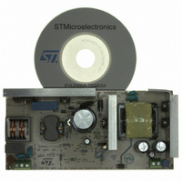
Manufacturer Part Number
EVL6566A-75WES4
Description
BOARD DEMO FOR L6563/LL6566A
Manufacturer
STMicroelectronics
Type
Power Factor Correctionr
Specifications of EVL6566A-75WES4
Main Purpose
AC/DC, Primary and Secondary Side with PFC
Outputs And Type
1, Isolated
Power - Output
75W
Voltage - Output
19V
Current - Output
4A
Voltage - Input
90 ~ 264VAC
Regulator Topology
Flyback
Board Type
Fully Populated
Utilized Ic / Part
L6563, L6566A, TSM1014
Input Voltage
90 V to 264 V
Output Voltage
19 V
Dimensions
78 mm x 170 mm
Product
Power Management Modules
Lead Free Status / RoHS Status
Lead free / RoHS Compliant
Frequency - Switching
-
Lead Free Status / Rohs Status
Lead free / RoHS Compliant
For Use With/related Products
L6563S, L6566A
Other names
497-8834
Available stocks
Company
Part Number
Manufacturer
Quantity
Price


Application information
5.13
Note:
40/51
the base terminal are several ten kW) but this could distort the signal on the MULT pin of the
PFC chip and adversely affect the operation of the pre-regulator. C
capacitor (in the μF) to have small residual ripple superimposed on the dc level; as a rule-of-
thumb, use a time constant (R
then fine tune if needed, considering also transient conditions such as mains missing
cycles.
If temperature effects are critical, the NPN Q can be replaced by a PNP-NPN pair arranged
as shown in
adopted anyway.
The voltage on the pin is clamped upwards at about 3.15 V; then, if the function is not used
the pin has to be connected to Vcc through a resistor (220 to 680 kΩ).
Slope compensation
The pin MODE/SC (12), when not connected to VREF, provides a voltage ramp during
MOSFET's ON-time synchronous to that of the internal oscillator sawtooth, with 0.8 mA
minimum current capability. This ramp is intended for implementing additive slope
compensation on current sense. This is needed to avoid the sub-harmonic oscillation that
arises in all peak-current-mode-controlled converters working at fixed frequency in
continuous conduction mode with a duty cycle close to or exceeding 50 %.
Figure 27. Slope compensation waveforms
The compensation will be realized by connecting a programming resistor between this pin
and the current sense input (pin 7, CS). The CS pin has to be connected to the sense
resistor with another resistor to make a summing node on the pin. Since no ramp is
delivered during MOSFET OFF-time (see
programming resistor is needed to ensure a clean operation at light loads.
The addition of the slope compensation ramp will reduce the available dynamics of the
current signal; thereby, the value of the sense resistor must be determined taking this into
account. Note also that the burst-mode threshold (in terms of power) will be slightly
changed.
If slope compensation is not required with FF operation, the pin shall be left floating.
Figure 26 on page 39
MODE/SC
oscillator
(pin 12)
Internal
(pin 4)
GD
L
+ R
on the right-hand side; other sensing techniques can be
H
)·C
F
at least 4-5 times the maximum line cycle period,
Figure 27
), no external component other than the
F
needs to be quite a big
t
t
t
L6566A
Related parts for EVL6566A-75WES4
Image
Part Number
Description
Manufacturer
Datasheet
Request
R

Part Number:
Description:
BOARD EVAL FOR L6566A
Manufacturer:
STMicroelectronics
Datasheet:

Part Number:
Description:
STMicroelectronics [RIPPLE-CARRY BINARY COUNTER/DIVIDERS]
Manufacturer:
STMicroelectronics
Datasheet:
Part Number:
Description:
STMicroelectronics [LIQUID-CRYSTAL DISPLAY DRIVERS]
Manufacturer:
STMicroelectronics
Datasheet:

Part Number:
Description:
BOARD EVAL FOR MEMS SENSORS
Manufacturer:
STMicroelectronics
Datasheet:
Part Number:
Description:
NPN TRANSISTOR POWER MODULE
Manufacturer:
STMicroelectronics
Datasheet:
Part Number:
Description:
TURBOSWITCH ULTRA-FAST HIGH VOLTAGE DIODE
Manufacturer:
STMicroelectronics
Datasheet:
Part Number:
Description:
Manufacturer:
STMicroelectronics
Datasheet:
Part Number:
Description:
DIODE / SCR MODULE
Manufacturer:
STMicroelectronics
Datasheet:
Part Number:
Description:
DIODE / SCR MODULE
Manufacturer:
STMicroelectronics
Datasheet:
Part Number:
Description:
Search -----> STE16N100
Manufacturer:
STMicroelectronics
Datasheet:
Part Number:
Description:
Search ---> STE53NA50
Manufacturer:
STMicroelectronics
Datasheet:
Part Number:
Description:
NPN Transistor Power Module
Manufacturer:
STMicroelectronics
Datasheet: