HW-SD1800A-DSP-SB-UNI-G Xilinx Inc, HW-SD1800A-DSP-SB-UNI-G Datasheet - Page 12
HW-SD1800A-DSP-SB-UNI-G
Manufacturer Part Number
HW-SD1800A-DSP-SB-UNI-G
Description
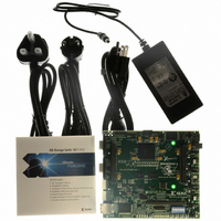
KIT DEVELOPMENT SPARTAN 3ADSP
Manufacturer
Xilinx Inc
Series
Spartan™-3A DSPr
Type
DSPr
Datasheet
1.HW-SD1800A-DSP-SB-UNI-G.pdf
(38 pages)
Specifications of HW-SD1800A-DSP-SB-UNI-G
Contents
Development Platform, Power Supply and software
Silicon Manufacturer
Xilinx
Features
10/100/1000 PHY, JTAG Programming And Configuration Port
Silicon Family Name
Spartan-3A
Silicon Core Number
3SD1800A-FG676
Lead Free Status / RoHS Status
Lead free / RoHS Compliant
For Use With/related Products
Spartan 3A
Lead Free Status / RoHS Status
Lead free / RoHS Compliant, Lead free / RoHS Compliant
Other names
122-1574
HW-SD1800A-DSP-DB-UNI-G
HW-SD1800A-DSP-DB-UNI-G
HW-SD1800A-DSP-SB-UNI-G
HW-SD1800A-DSP-DB-UNI-G
HW-SD1800A-DSP-DB-UNI-G
HW-SD1800A-DSP-SB-UNI-G
Available stocks
Company
Part Number
Manufacturer
Quantity
Price


Functional Description
36
Intel J3 Parallel Flash
Table 3: FPGA DDR2 Interface Pinout (Cont’d)
The Flash memory consists of a single J3 Flash device in a TSOP-56 package and connected
to the dedicated BPI configuration port of the FPGA. The Intel JS28F128J3D is a 128-Mbit
device organized as 16-Mbit x 8. The installed J3 device supports asynchronous memory
accesses at a 75 nanosecond access time. The Flash interface is split across two banks, with
all but the 8 data bits connected to Bank 1 (3.3V), and the 8 data bits connected to Bank 2.
Because Bank 2 may be set to either 2.5V or 3.3V, the 8 Flash data bits are interfaced to Bank
2 via a Texas Instruments SN74AVC8T245 dual-supply bus transceiver with the Flash
Write Enable (FLASH_WE#) signal controlling transceiver direction and the Flash chip
select signal (FLASH_CS) enabling the transceiver. The maximum propagation delay of
2.9 nanoseconds through this transceiver is not significant with the 75 nanosecond Flash
access time. Jumper JP1 may be used to write-protect the Flash memory by placing a shunt
across pins 2 and 3. Default setting is JP1 1:2.
interface pinout.
FPGA_DDR_UDQS_#_1
FPGA_DDR_LDQS_#_1
FPGA_DDR_UDQS_#0
FPGA_DDR_LDQS_#0
FPGA_DDR_UDQS_0
FPGA_DDR_UDQS_1
FPGA_DDR_LDQS_0
FPGA_DDR_LDQS_1
FPGA_DDR_CLK_0#
FPGA_DDR_CLK_1#
RST_DQS_DIV (out)
FPGA_DDR_CLK_0
FPGA_DDR_CLK_1
RST_DQS_DIV (in)
MB_FB_CLK (out)
MB_FB_CLK (in)
DDR2 Signal
www.xilinx.com
FPGA Pin
Number
T10
M2
W3
W4
N1
N2
N5
N4
N7
V7
V6
U4
T9
T5
R2
R4
Table 4
Spartan-3A DSP Starter Platform User Guide
FPGA_DDR_D15
FPGA_DDR_D16
FPGA_DDR_D17
FPGA_DDR_D18
FPGA_DDR_D19
FPGA_DDR_D20
FPGA_DDR_D21
FPGA_DDR_D22
FPGA_DDR_D23
FPGA_DDR_D24
FPGA_DDR_D25
FPGA_DDR_D26
FPGA_DDR_D27
FPGA_DDR_D28
FPGA_DDR_D29
FPGA_DDR_D30
FPGA_DDR_D31
DDR2 Signal
details the Parallel Flash FPGA
UG454 (v1.1) January 30, 2009
FPGA Pin Number
P10
U1
U2
N9
V5
R8
R7
R5
R6
P8
P9
P7
P6
T3
T4
P4
P3
R
Related parts for HW-SD1800A-DSP-SB-UNI-G
Image
Part Number
Description
Manufacturer
Datasheet
Request
R

Part Number:
Description:
KIT DEVELOPMENT SPARTAN 3ADSP
Manufacturer:
Xilinx Inc

Part Number:
Description:
IC CPLD .8K 36MCELL 44-VQFP
Manufacturer:
Xilinx Inc
Datasheet:

Part Number:
Description:
IC CPLD 72MCRCELL 10NS 44VQFP
Manufacturer:
Xilinx Inc
Datasheet:

Part Number:
Description:
IC CPLD 1.6K 72MCELL 64-VQFP
Manufacturer:
Xilinx Inc
Datasheet:

Part Number:
Description:
IC CR-II CPLD 64MCELL 44-VQFP
Manufacturer:
Xilinx Inc
Datasheet:

Part Number:
Description:
IC CPLD 1.6K 72MCELL 100-TQFP
Manufacturer:
Xilinx Inc
Datasheet:

Part Number:
Description:
IC CR-II CPLD 64MCELL 56-BGA
Manufacturer:
Xilinx Inc
Datasheet:

Part Number:
Description:
IC CPLD 72MCRCELL 7.5NS 44VQFP
Manufacturer:
Xilinx Inc
Datasheet:
Part Number:
Description:
IC CR-II CPLD 64MCELL 100-VQFP
Manufacturer:
Xilinx Inc
Datasheet:
Part Number:
Description:
IC CPLD 1.6K 72MCELL 100-TQFP
Manufacturer:
Xilinx Inc
Datasheet:

Part Number:
Description:
IC CPLD 72MCRCELL 7.5NS 64VQFP
Manufacturer:
Xilinx Inc
Datasheet:
Part Number:
Description:
IC CPLD 1.6K 72MCELL 100-TQFP
Manufacturer:
Xilinx Inc
Datasheet:

Part Number:
Description:
IC CPLD 1.5K 64MCELL HP 44-VQFP
Manufacturer:
Xilinx Inc

Part Number:
Description:
IC CPLD 36MCRCELL 15NS 44PLCC
Manufacturer:
Xilinx Inc
Datasheet:

Part Number:
Description:
IC CPLD 36MCRCELL 10NS 44PLCC
Manufacturer:
Xilinx Inc
Datasheet: