MPC8360E-RDK Freescale Semiconductor, MPC8360E-RDK Datasheet - Page 23
MPC8360E-RDK
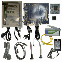
Manufacturer Part Number
MPC8360E-RDK
Description
BOARD REFERENCE DESIGN FOR MPC
Manufacturer
Freescale Semiconductor
Series
PowerQUICC II™ PROr
Type
MPUr
Specifications of MPC8360E-RDK
Contents
Board, Cables, CD, Power Supply
Processor To Be Evaluated
MPC8360E
Data Bus Width
32 bit
Interface Type
RS-232, Ethernet, USB
Operating Supply Voltage
1.3 V
For Use With/related Products
MPC8360E
Lead Free Status / RoHS Status
Lead free / RoHS Compliant


Figure 6
6.2.2
Table 21
DDR and DDR2 SDRAM interface.
Freescale Semiconductor
At recommended operating conditions with GV
At recommended operating conditions with GV
MDQS—MDQ/MECC input skew per byte
Notes:
1. AC timing values are based on the DDR data rate, which is twice the DDR memory bus frequency.
2. Maximum possible skew between a data strobe (MDQS[n]) and any corresponding bit of data (MDQ[8n + {0...7}] if 0 ≤ n ≤ 7)
MCK[n] cycle time, (MCK[n]/MCK[n] crossing)
Skew between any MCK to ADDR/CMD
or ECC (MECC[{0...7}] if n = 8).
MPC8360E/MPC8358E PowerQUICC II Pro Processor Revision 2.x TBGA Silicon Hardware Specifications, Rev. 4
MDQS[n]
MDQ[x]
shows the input timing diagram for the DDR controller.
and
MCK[n]
MCK[n]
DDR and DDR2 SDRAM Output AC Timing Specifications
Table 22
Table 21. DDR and DDR2 SDRAM Output AC Timing Specifications for Source
Parameter
Table 20. DDR and DDR2 SDRAM Input AC Timing Specifications Mode
Parameter
provide the output AC timing specifications and measurement conditions for the
8
333 MHz
266 MHz
200 MHz
DD
DD
Figure 6. DDR Input Timing Diagram
of (1.8 or 2.5 V) ± 5%.
of (1.8 V or 2.5 V) ± 5%.
333 MHz
266 MHz
200 MHz
t
t
MCK
Symbol
DISKEW
t
DISKEW
Synchronous Mode
Symbol
t
AOSKEW
t
MCK
1
D0
–1125
–1250
–750
Min
D1
–1.0
–1.1
–1.2
Min
6
t
DISKEW
1125
1250
Max
750
Max
0.2
0.3
0.4
10
DDR and DDR2 SDRAM
Unit
ps
Unit
ns
ns
Notes
Notes
1, 2
2
3
23
Related parts for MPC8360E-RDK
Image
Part Number
Description
Manufacturer
Datasheet
Request
R

Part Number:
Description:
Mpc8360e Powerquicc Ii Pro Family
Manufacturer:
Freescale Semiconductor, Inc
Datasheet:

Part Number:
Description:
BOARD PROCESSOR FOR MPC8360E
Manufacturer:
Freescale Semiconductor
Datasheet:
Part Number:
Description:
Manufacturer:
Freescale Semiconductor, Inc
Datasheet:
Part Number:
Description:
Manufacturer:
Freescale Semiconductor, Inc
Datasheet:
Part Number:
Description:
Manufacturer:
Freescale Semiconductor, Inc
Datasheet:
Part Number:
Description:
Manufacturer:
Freescale Semiconductor, Inc
Datasheet:
Part Number:
Description:
Manufacturer:
Freescale Semiconductor, Inc
Datasheet:
Part Number:
Description:
Manufacturer:
Freescale Semiconductor, Inc
Datasheet:
Part Number:
Description:
Manufacturer:
Freescale Semiconductor, Inc
Datasheet:
Part Number:
Description:
Manufacturer:
Freescale Semiconductor, Inc
Datasheet:
Part Number:
Description:
Manufacturer:
Freescale Semiconductor, Inc
Datasheet:
Part Number:
Description:
Manufacturer:
Freescale Semiconductor, Inc
Datasheet:
Part Number:
Description:
Manufacturer:
Freescale Semiconductor, Inc
Datasheet:
Part Number:
Description:
Manufacturer:
Freescale Semiconductor, Inc
Datasheet:
Part Number:
Description:
Manufacturer:
Freescale Semiconductor, Inc
Datasheet: