AD9433/PCB Analog Devices Inc, AD9433/PCB Datasheet - Page 18
AD9433/PCB
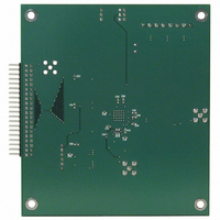
Manufacturer Part Number
AD9433/PCB
Description
BOARD EVAL FOR AD9433
Manufacturer
Analog Devices Inc
Datasheet
1.AD9433BSVZ-105.pdf
(20 pages)
Specifications of AD9433/PCB
Rohs Status
RoHS non-compliant


AD9433
ANALOG INPUT
The analog input to the AD9433 is a differential buffer. The
input buffer is self-biased by an on-chip resistor divider that
sets the dc common-mode voltage to a nominal 4 V (see the
Equivalent Circuits section). Rated performance is achieved
by driving the input differentially. The minimum input offset
voltage is obtained when driving from a source with a low
differential source impedance, such as a transformer in ac
applications (see Figure 45). Capacitive coupling at the inputs
increases the input offset voltage by as much as 50 mV.
In the highest frequency applications, two transformers con-
nected in series may be necessary to minimize even-order
harmonic distortion. The first transformer isolates and converts
the signal to a differential signal, but the grounded input on the
primary side degrades amplitude balance on the secondary
winding. Capacitive coupling between the windings causes
this imbalance. Because one input to the first transformer is
grounded, there is little or no capacitive coupling, resulting in
an amplitude mismatch at the output of the first transformer. A
second transformer improves the amplitude balance, and thus
improves the harmonic distortion. A wideband transformer,
such as the ADT1-1WT from Mini-Circuits®, is recommended
for these applications, because the bandwidth through the two
transformers is reduced by √2.
Driving the ADC single-ended degrades performance, partic-
ularly even-order harmonics. For best dynamic performance,
impedances at AIN and AIN should match. Special care was
taken in the design of the analog input section of the AD9433
to prevent damage and corruption of data when the input is
overdriven.
SFDR OPTIMIZATION
When set to Logic 1, the SFDR MODE pin enables a proprietary
circuit that can improve the spurious-free dynamic range (SFDR)
performance of the AD9433. This pin is useful in applications
where the dynamic range of the system is limited by discrete
spurious frequency content caused by nonlinearities in the
ADC transfer function.
Figure 46. Driving the Analog Input with Two Transformers for Improved
ANALOG
SOURCE
SIGNAL
50Ω
ANALOG
SOURCE
SIGNAL
Figure 45. Transformer-Coupled Analog Input Circuit
50Ω
1:1
Even-Order Harmonics
1:1
1:1
25Ω
25Ω
25Ω
25Ω
0.1µF
0.1µF
AIN
AIN
AD9433
AIN
AIN
AD9433
Rev. A | Page 18 of 20
Enabling this circuit gives the circuit a dynamic transfer functi
meaning that the voltage t
codes can change from clock cycle to clock cycle. While improving
spurious frequency content, this dynamic aspect of the transfer
function may be inappropriate for some time domain applications
of the converter. Connecting the SFDR MODE pin to ground
disables this function. The improvement in the linearity of the
converter and its effect on spurious free dynamic range is shown
in Figure 4 and Figure 5 and in Figure 22 and Figure 23.
DIGITAL OUTPUTS
The digital outputs are 3 V (2.7 V to 3.3 V) TTL-/CMOS-
compatible for lower pow
format is selectable through the data format select (DFS)
CMOS input. DFS = 1 selects offset binary; DFS = 0 selects
twos complement coding (see Table 8 and Table 9).
Table 8. Offset Binary Output Coding (DFS = 1, V
Code
4095
…
2048
2047
…
0
Table 9. Twos Comple
(D
Code
+2047
…
0
−1
…
−2048
VOLTAGE RE
A stable
AD9433 (VREFOUT). In nor
ence is used by strapping Pin 45 to Pin 46 and placing a 0.1 μF
decoupling capacitor at VREFIN. The input range can be adjusted
by varying the reference voltage applied to the AD9433. No appre-
ciable degradation in performance occurs when the reference is
adjusted ±5%. The full-scale range of the ADC tracks reference
voltage changes linearly.
TIMING
The AD9433 provides latc
delays. Dat
after the rising edge of the encode command (see Figure 2). T
length of the output data lines and the loads placed on them
should be minimized to reduce transients within the AD9433;
these transients can detract from the dynamic performance of
the converter. The minimum guaranteed conversion rate of the
AD9433 is 10 MSPS. At internal clock rates below 10 MSPS,
dynamic performance may degrade.
FS = 0, V
and acc
a outputs are available one propagation delay (t
REF
=
urate 2.5
FER
AIN − AIN (V)
+1.000
…
0
−0.0
…
−1.000
AIN − AIN (V)
+1.000
…
0
−0.00049
…
−1.000
2.5 V)
0049
ENCE
me
V voltage refer
er consumption. The output data
hreshold between two adjacent output
hed data outputs, with 10 pipeline
nt Output C
mal operation, the internal refer-
oding
ence is built into t
Digital Output
1111 1111 1111
…
1000 0000 0000
011
…
0000 0000 0000
Digital Output
0111 1111 1111
…
0000 0000 0000
111
…
1000 0000 0000
1 1111 1111
1 1111 1111
REF
= 2.5
he
PD
)
on,
V)
he
Related parts for AD9433/PCB
Image
Part Number
Description
Manufacturer
Datasheet
Request
R

Part Number:
Description:
±1.7g Dual-Axis IMEMS Accelerometer Evaluation Board
Manufacturer:
Analog Devices Inc
Datasheet:

Part Number:
Description:
Inertial Sensor Evaluation System
Manufacturer:
Analog Devices Inc
Datasheet:
Part Number:
Description:
Manufacturer:
Analog Devices Inc
Datasheet:
Part Number:
Description:
Manufacturer:
Analog Devices Inc
Datasheet:
Part Number:
Description:
Manufacturer:
Analog Devices Inc
Datasheet:
Part Number:
Description:
Manufacturer:
Analog Devices Inc
Datasheet:
Part Number:
Description:
Manufacturer:
Analog Devices Inc
Datasheet:
Part Number:
Description:
Manufacturer:
Analog Devices Inc
Datasheet:
Part Number:
Description:
Manufacturer:
Analog Devices Inc
Datasheet:
Part Number:
Description:
Manufacturer:
Analog Devices Inc
Datasheet:
Part Number:
Description:
Manufacturer:
Analog Devices Inc
Datasheet:
Part Number:
Description:
Manufacturer:
Analog Devices Inc
Datasheet:
Part Number:
Description:
Manufacturer:
Analog Devices Inc
Datasheet: