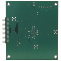
AD9433/PCB Analog Devices Inc, AD9433/PCB Datasheet - Page 19

AD9433/PCB
Manufacturer Part Number
AD9433/PCB
Description
BOARD EVAL FOR AD9433
Manufacturer
Analog Devices Inc
Datasheet
1.AD9433BSVZ-105.pdf
(20 pages)
Specifications of AD9433/PCB
Rohs Status
RoHS non-compliant
APPLICATIONS INFORMATION
LAYOUT INFORMATION
A multilayer board is recommended to achieve best results. It is
highly recommended that high quality, ceramic chip capacitors be
used to decouple each supply pin to ground directly at the device.
The pinout of the AD9433 facilitates ease of use in the imple-
mentation of high frequency, high resolution design practices.
All of the digital outputs and their supply and ground pin
connections are segregated on one side of the package, with
the inputs on the opposite side for isolation purposes.
Care should be taken when routing the digital output traces.
To prevent coupling through the digital outputs into the analog
portion of the AD9433 (V
loading should be placed on these outputs.
It is recommended that a fanout of only one gate be used for all
AD9433 digital outputs.
The layout of the encode circuit is equally critical and should be
treated as an analog input. Any noise received on this circuitry
results in corruption in the digitization process and lower over-
all performance. The encode clock must be isolated from the
digital outputs and the analog inputs.
CC
, AIN, and VREF), minimal capacitive
Rev. A | Page 19 of 20
REPLACING THE AD9432 WITH THE AD9433
The AD9433 is pin-compatible with the AD9432, although there
are two control pins on the AD9433 that are do not connect (DNC)
and supply (V
Table 10. AD9432/AD9433 Pin Differences
Pin
41
42
Using the AD9433 in an AD9432 pin assignment configures the
AD9433 as follows:
•
•
Table 11 summarizes the differences between the AD9432 and
AD9433 analog and encode input common-mode voltages.
These inputs can be ac-coupled so that the devices can be used
interchangeably.
Table 11. AD9432/AD9433 Analog and Encode Input
Common-Mode Voltages
Input Pins
ENCODE/ENCODE
AIN/AIN
The SFDR improvement circuit is enabled.
The DFS pin floats low, selecting twos complement coding
for the digital outputs. (Twos complement coding is the
only output coding available on the AD9432.)
AD9432
DNC
V
CC
CC
) connections on the AD9432 (see Table 10).
AD9432
1.6 V
3.0 V
Common-Mode Voltage
AD9433
DFS
SFDR MODE
AD9433
3.75 V
4.0 V
AD9433


