AD9433/PCB Analog Devices Inc, AD9433/PCB Datasheet - Page 5
AD9433/PCB
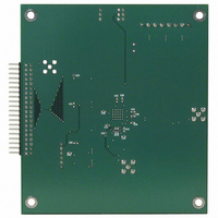
Manufacturer Part Number
AD9433/PCB
Description
BOARD EVAL FOR AD9433
Manufacturer
Analog Devices Inc
Datasheet
1.AD9433BSVZ-105.pdf
(20 pages)
Specifications of AD9433/PCB
Rohs Status
RoHS non-compliant


SWITCHING SPECIFICATIONS
V
Table 3.
Parameter
Encode Rate
Encode Pulse Width High (t
Encode Pulse Width Low (t
Aperture Delay (t
Aperture Uncertainty (Jitter)
Output Valid Time (t
Output Propagation Delay (t
Output Rise Time (t
Output Fall Time (t
Out-of-Range Recovery Time
Transient Response Time
Latency
1
2
TIMING DIAGRAM
Aperture uncertainty includes contribution of the AD9433, crystal clock reference, and encode drive circuit.
t
to exceed an ac load of 10 pF or a dc current of 50 μA. Rise and fall times are measured from 10% to 90%.
V
DD
and t
= 3.3 V, V
PD
are measured from the transition points of the ENCODE input to the 50%/50% levels of the digital output swing. The digital output load during testing is not
D11 TO D0
CC
AIN
= 5 V; differential encode input, unless otherwise noted.
A
)
ENCODE
ENCODE
F
R
)
V
)
2
2
)
2
SAMPLE N – 1
EL
EH
)
PD
1
)
)
2
DATA N – 11
SAMPLE N
t
A
t
Temp
Full
Full
Full
25°C
25°C
Full
Full
Full
Full
25°C
Full
EH
25°C
DATA N – 10
t
EL
SAMPLE N + 1
Test
Level
IV
IV
IV
V
V
VI
VI
V
V
V
V
IV
Figure 2. Timing Diagram
Rev. A | Page 5 of 20
DATA
N – 9
Min
10
2.9
2.9
2.5
DATA
N – 2
SAMPLE N + 8
105 MSPS
Typ
2.1
0.25
4.0
4.0
2.1
1.9
2
2
10
DATA N – 1
SAMPLE N + 9
t
Max
105
5.5
PD
DATA N
Min
10
2.4
2.4
2.5
SAMPLE N + 10
125 MSPS
t
V
Typ
2.1
0.25
4.0
4.0
2.1
1.9
2
2
10
1/
DATA N + 1
f
S
Max
125
5.5
AD9433
Unit
ns
ns
ns
ps rms
Cycles
MSPS
ns
ns
ns
ns
ns
ns
Related parts for AD9433/PCB
Image
Part Number
Description
Manufacturer
Datasheet
Request
R

Part Number:
Description:
±1.7g Dual-Axis IMEMS Accelerometer Evaluation Board
Manufacturer:
Analog Devices Inc
Datasheet:

Part Number:
Description:
Inertial Sensor Evaluation System
Manufacturer:
Analog Devices Inc
Datasheet:
Part Number:
Description:
Manufacturer:
Analog Devices Inc
Datasheet:
Part Number:
Description:
Manufacturer:
Analog Devices Inc
Datasheet:
Part Number:
Description:
Manufacturer:
Analog Devices Inc
Datasheet:
Part Number:
Description:
Manufacturer:
Analog Devices Inc
Datasheet:
Part Number:
Description:
Manufacturer:
Analog Devices Inc
Datasheet:
Part Number:
Description:
Manufacturer:
Analog Devices Inc
Datasheet:
Part Number:
Description:
Manufacturer:
Analog Devices Inc
Datasheet:
Part Number:
Description:
Manufacturer:
Analog Devices Inc
Datasheet:
Part Number:
Description:
Manufacturer:
Analog Devices Inc
Datasheet:
Part Number:
Description:
Manufacturer:
Analog Devices Inc
Datasheet:
Part Number:
Description:
Manufacturer:
Analog Devices Inc
Datasheet: