AD9433/PCB Analog Devices Inc, AD9433/PCB Datasheet - Page 7
AD9433/PCB
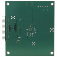
Manufacturer Part Number
AD9433/PCB
Description
BOARD EVAL FOR AD9433
Manufacturer
Analog Devices Inc
Datasheet
1.AD9433BSVZ-105.pdf
(20 pages)
Specifications of AD9433/PCB
Rohs Status
RoHS non-compliant


PIN CONFIGURATION AND FUNCTION DESCRIPTIONS
Table 6. Pin Function Descriptions
Pin No.
1, 3, 4, 9, 11, 33,
34, 35, 38, 39, 40,
43, 48, 51
2, 5, 6, 10, 36, 37,
44, 47, 52
7
8
12, 21, 24, 31
13, 22, 23, 32
14
15 to 20, 25 to 30
41
42
45
46
49
50
Mnemonic
GND
V
ENCODE
ENCODE
DGND
V
OR
D11 to D6, D5 to D0
DFS
SFDR MODE
VREFIN
VREFOUT
AIN
AIN
Exposed Pad (EP)
CC
DD
ENCODE
ENCODE
NOTES
1. THE EXPOSED PADDLE ON THE UNDERSIDE OF THE PACKAGE MUST
PADDLE TO THE PCB INCREASES THE RELIABILITY OF THE SOLDER
BE SOLDERED TO THE GROUND PLANE. SOLDERING THE EXPOSED
JOINTS, MAXIMIZING THE THERMAL CAPABILITY OF THE PACKAGE.
DGND
GND
GND
GND
GND
GND
V
V
V
V
V
Description
Analog Ground.
Analog Supply (5 V).
Encode Clock for ADC, Complementary.
Encode Clock for ADC, True. ADC samples on rising edge of ENCODE.
Digital Output Ground.
Digital Output Power Supply (3 V).
Out-of-Range Output.
Digital Output.
Data Format Select. Logic low = twos complement, logic high = offset binary; floats low.
CMOS Control Pin. This pin enables SFDR mode, a proprietary circuit that can improve the SFDR
performance of the AD9433. SFDR mode is useful in applications where the dynamic range of
the system is limited by discrete spurious frequency content caused by nonlinearities in the
ADC transfer function. Set this pin to 0 for normal operation; floats low.
Reference Input for ADC (2.5 V Typical). Bypass with 0.1 μF capacitor to ground.
Internal Reference Output (2.5 V Typical).
Analog Input, True.
Analog Input, Complementary.
The exposed paddle on the underside of the package must be soldered to the ground plane.
Soldering the exposed paddle to the PCB increases the reliability of the solder joints, maximiz-
ing the thermal capability of the package.
CC
CC
CC
CC
DD
10
11
12
13
1
2
3
4
5
6
7
8
9
52 51 50 49 48 47 46 45 44 43 42 41 40
14 15 16 17 18 19 20 21 22 23 24 25 26
PIN 1
Figure 3. Pin Configuration
Rev. A | Page 7 of 20
(Not to Scale)
AD9433
TOP VIEW
39
38
37
36
35
34
33
32
31
30
29
28
27
GND
GND
V
V
GND
GND
GND
V
DGND
D0 (LSB)
D1
D2
D3
CC
CC
DD
AD9433
Related parts for AD9433/PCB
Image
Part Number
Description
Manufacturer
Datasheet
Request
R

Part Number:
Description:
±1.7g Dual-Axis IMEMS Accelerometer Evaluation Board
Manufacturer:
Analog Devices Inc
Datasheet:

Part Number:
Description:
Inertial Sensor Evaluation System
Manufacturer:
Analog Devices Inc
Datasheet:
Part Number:
Description:
Manufacturer:
Analog Devices Inc
Datasheet:
Part Number:
Description:
Manufacturer:
Analog Devices Inc
Datasheet:
Part Number:
Description:
Manufacturer:
Analog Devices Inc
Datasheet:
Part Number:
Description:
Manufacturer:
Analog Devices Inc
Datasheet:
Part Number:
Description:
Manufacturer:
Analog Devices Inc
Datasheet:
Part Number:
Description:
Manufacturer:
Analog Devices Inc
Datasheet:
Part Number:
Description:
Manufacturer:
Analog Devices Inc
Datasheet:
Part Number:
Description:
Manufacturer:
Analog Devices Inc
Datasheet:
Part Number:
Description:
Manufacturer:
Analog Devices Inc
Datasheet:
Part Number:
Description:
Manufacturer:
Analog Devices Inc
Datasheet:
Part Number:
Description:
Manufacturer:
Analog Devices Inc
Datasheet: