AD9549/PCBZ Analog Devices Inc, AD9549/PCBZ Datasheet - Page 27
AD9549/PCBZ
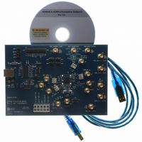
Manufacturer Part Number
AD9549/PCBZ
Description
BOARD EVALUATION FOR AD9549
Manufacturer
Analog Devices Inc
Datasheet
1.AD9549ABCPZ.pdf
(76 pages)
Specifications of AD9549/PCBZ
Main Purpose
Timing, Clock Generator
Embedded
No
Utilized Ic / Part
AD9549
Primary Attributes
2 Inputs, 2 Outputs, VCO
Secondary Attributes
CMOS, HSTL Output Logic, Graphical User Interface
Lead Free Status / RoHS Status
Lead free / RoHS Compliant


The following four values are needed to calculate the correct
values of the reference monitor:
•
•
•
•
The monitor window size is the difference between the maximum
and minimum number of counts accumulated between adjacent
edges of the reference input. If this window is too small, random
variations cause the OOL detector to indicate incorrectly that
a reference is out of limits. However, the time required to
determine if the reference frequency is valid increases with window
size. A window size of at least 20 is a good starting point.
The four input values mentioned previously are used to calculate
the OOL divider (D) and OOL nominal value (N), which, in
turn, are used to calculate the OOL upper limit (U) and OOL
lower limit (L), according to the following formulas:
The timing accuracy is dependent on two factors. The first is
the inherent accuracy of f
the reference monitor. As such, the accuracy of the reference
monitor can be no better than the accuracy of f
factor is the value of W, which must be sufficiently large (≥20)
so that the timer resolves the deviation between a nominal value
of f
As an example, let f
W = 20. The limits are then
Next, let Ε = 0.0005%. Then the limits are
Note that the number of counts (and time) required to make
this measurement has increased by 100×. In addition, it is
recommended that D be an odd number.
R
System clock frequency, f
Reference input frequency, f
Error bound, E (1% = 0.01)
Monitor window size (W)
and a value that is out of limits.
D = 79
Lower Limit = 1980
Upper Limit = 2020
D = 7999
Lower Limit = 199980
Upper Limit = 200020
U
D
N
L
=
=
=
=
max
floor(
ceil(
f
f
S
R
×
N
, 1
D
4
N
)
min
)
+
−
R
floor(
= 10 MHz, Ε = 0.05%, f
floor(
65
,
535
S
W
W
because it serves as the time base for
)
,
S
ceil
)
(usually 1 GHz)
R
(in Hz)
1
5
×
f
f
R
S
×
W
E
S
= 1 GHz, and
S
. The second
Rev. D | Page 27 of 76
REFERENCE SWITCHOVER
The AD9549 supports dual input reference clocks. Reference
switchover can be accomplished either automatically or manually
by appropriately programming the automatic selector bit in the
I/O register map (Register 0x01C0, Bit 2).
Transition to a newly selected reference depends on a number
of factors:
•
•
•
•
A functional diagram of the reference switchover and holdover
logic is shown in Figure 33.
In manual mode, the active reference is determined by an exter-
nally applied logic level to the REFSELECT pin. In automatic
mode, an internal state machine determines which reference is
active, and the REFSELECT pin becomes an output indicating
which reference the state machine is using.
The user can override the active reference chosen by the internal
state machine via the enable ref input override bit. The REF_AB
bit is then used to select the desired reference. When in override,
it is important to note that the REFSELECT pin does not
indicate the physical reference selected by the REF_AB bit.
Instead, it indicates the reference that the internal state machine
would select if the device were not in the override mode. This
allows the user to force a reference switchover by means of the
programming registers while monitoring the response of the
state machine via the REFSELECT pin.
The same type of operation (manual/automatic and override)
also applies to the holdover function, as shown in the reference
switchover logic diagram (see Figure 33). The dashed arrows in
the diagram indicate that the state machine output is available
to the REFSELECT and HOLDOVER pins when in override mode.
State of the REFSELECT pin
State of the REF_AB bit (Register 0x01C1[2])
State of the enable ref input override bit (Register 0x01C1[3])
Holdover status
MACHINE
STATE
Figure 33. Reference Switchover and Holdover Logic
REFSEL STATE
ACTIVE HOLDOVER STATE
REFSELECT
HOLDOVER
ACTIVE REFSEL STATE
HOLDOVER
DERIVED
DERIVED
STATE
AUTOREFSEL
AUTOHOLD
0
1
1
0
HLDOVR
REF_AB
OVERRIDE HLDPIN
OVERRIDE REFPIN
0
1
1
0
TO
REFERENCE
SWITCHING
CONTROL
LOGIC
TO
HOLDOVER
CONTROL
LOGIC
AD9549
Related parts for AD9549/PCBZ
Image
Part Number
Description
Manufacturer
Datasheet
Request
R


Part Number:
Description:
±1.7g Dual-Axis IMEMS Accelerometer Evaluation Board
Manufacturer:
Analog Devices Inc
Datasheet:

Part Number:
Description:
Inertial Sensor Evaluation System
Manufacturer:
Analog Devices Inc
Datasheet:
Part Number:
Description:
Manufacturer:
Analog Devices Inc
Datasheet:
Part Number:
Description:
Manufacturer:
Analog Devices Inc
Datasheet:
Part Number:
Description:
Manufacturer:
Analog Devices Inc
Datasheet:
Part Number:
Description:
Manufacturer:
Analog Devices Inc
Datasheet:
Part Number:
Description:
Manufacturer:
Analog Devices Inc
Datasheet:
Part Number:
Description:
Manufacturer:
Analog Devices Inc
Datasheet:
Part Number:
Description:
Manufacturer:
Analog Devices Inc
Datasheet:
Part Number:
Description:
Manufacturer:
Analog Devices Inc
Datasheet:
Part Number:
Description:
Manufacturer:
Analog Devices Inc
Datasheet:
Part Number:
Description:
Manufacturer:
Analog Devices Inc
Datasheet: