AD9549/PCBZ Analog Devices Inc, AD9549/PCBZ Datasheet - Page 35
AD9549/PCBZ
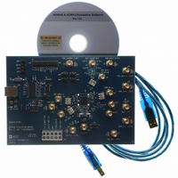
Manufacturer Part Number
AD9549/PCBZ
Description
BOARD EVALUATION FOR AD9549
Manufacturer
Analog Devices Inc
Datasheet
1.AD9549ABCPZ.pdf
(76 pages)
Specifications of AD9549/PCBZ
Main Purpose
Timing, Clock Generator
Embedded
No
Utilized Ic / Part
AD9549
Primary Attributes
2 Inputs, 2 Outputs, VCO
Secondary Attributes
CMOS, HSTL Output Logic, Graphical User Interface
Lead Free Status / RoHS Status
Lead free / RoHS Compliant


External Loop Filter (SYSCLK PLL)
The loop bandwidth of the SYSCLK PLL multiplier can be
adjusted by means of three external components, as shown in
Figure 44. The nominal gain of the VCO is 800 MHz/V. The
recommended component values are shown in Table 7. They
establish a loop bandwidth of approximately 1.6 MHz with
the charge pump current set to 250 μA. The default case is
N = 40 and assumes a 25 MHz SYSCLK input frequency and
generates an internal DAC sampling frequency (f
Table 7. Recommended Loop Filter Values for a Nominal
1.5 MHz SYSCLK PLL Loop Bandwidth
Multiplier
<8
10
20
40 (default)
60
Detail of SYSCLK Differential Inputs
A diagram of the SYSCLK input pins is provided in Figure 45.
Included are details of the internal components used to bias the
input circuitry. These components have a direct effect on the static
levels at the SYSCLK input pins. This information is intended to
aid in determining how best to interface to the device for a given
application.
Note that the SYSCLK PLL bypassed and SYSCLK PLL enabled
input paths are internally biased to a dc level of ~1 V. Care should
be taken to ensure that any external connections do not disturb
the dc bias because this may significantly degrade performance.
Generally, it is recommended that the SYSCLK inputs be
ac-coupled to the signal source (except when using a crystal
resonator).
HARMONIC SPUR REDUCTION
The most significant spurious signals produced by the DDS are
harmonically related to the desired output frequency of the DDS.
The source of these harmonic spurs can usually be traced to the
DAC, and the spur level is in the −60 dBc range. This ratio
AVDD
Figure 44. External Loop Filter for SYSCLK PLL
CHARGE
PUMP
FERRITE
R1
390 Ω
470 Ω
1 kΩ
2.2 kΩ
2.7 kΩ
BEAD
29
~2pF
AD9549
26
LOOP FILTER
Series C1
1 nF
820 pF
390 pF
180 pF
120 pF
C2
EXTERNAL
31
LOOP_FILTER
VCO
R1
C1
S
Shunt C2
82 pF
56 pF
27 pF
10 pF
5 pF
) of 1 GHz.
Rev. D | Page 35 of 76
represents a level that is about 10 bits below the full-scale
output of the DAC (10 bits down is 2
To reduce such a spur requires combining the original signal with
a replica of the spur, but offset in phase by 180°. This idea is the
foundation of the technique used to reduce harmonic spurs in
the AD9549. Because the DAC has 14-bit resolution, a −60 dBc
spur can be synthesized using only the lower four bits of the DAC
full-scale range. That is, the 4 LSBs can create an output level that
is approximately 60 dB below the full-scale level of the DAC
(commensurate with a −60 dBc spur). This fact gives rise to
a means of digitally reducing harmonic spurs or their aliased
images in the DAC output spectrum by digitally adding a sinusoid
at the input of the DAC with similar magnitude as the offending
spur but shifted in phase to produce destructive interference.
Although the worst spurs tend to be harmonic in origin, the fact
that the DAC is part of a sampled system results in the possibility
of some harmonic spurs appearing in nonharmonic locations in
the output spectrum. For example, if the DAC is sampled at 1 GHz
and generates an output sinusoid of 170 MHz, the fifth harmonic
would normally be at 850 MHz. However, because of the sampling
process, this spur appears at 150 MHz, only 20 MHz away from
the fundamental. Hence when attempting to reduce DAC spurs,
it is important to know the actual location of the harmonic spur
in the DAC output spectrum based on the DAC sample rate so
that its harmonic number can be reduced.
SYSCLKB
SYSCLK
Figure 45. Differential SYSCLK Inputs
MUX
V
V
SS
SS
~1.5pF
~1.5pF
AMP
~3pF
~3pF
CRYSTAL RESONATOR WITH
SYSCLK PLL BYPASSED
SYSCLK PLL ENABLED
SYSCLK PLL ENABLED
+
+
~1V
~1V
−10
, or 1/1024).
~2pF
~2pF
1kΩ
1kΩ
500Ω
500Ω
INTERNAL
CLOCK
INTERNAL
INTERNAL
CLOCK
CLOCK
AD9549
V
V
SS
SS
Related parts for AD9549/PCBZ
Image
Part Number
Description
Manufacturer
Datasheet
Request
R


Part Number:
Description:
±1.7g Dual-Axis IMEMS Accelerometer Evaluation Board
Manufacturer:
Analog Devices Inc
Datasheet:

Part Number:
Description:
Inertial Sensor Evaluation System
Manufacturer:
Analog Devices Inc
Datasheet:
Part Number:
Description:
Manufacturer:
Analog Devices Inc
Datasheet:
Part Number:
Description:
Manufacturer:
Analog Devices Inc
Datasheet:
Part Number:
Description:
Manufacturer:
Analog Devices Inc
Datasheet:
Part Number:
Description:
Manufacturer:
Analog Devices Inc
Datasheet:
Part Number:
Description:
Manufacturer:
Analog Devices Inc
Datasheet:
Part Number:
Description:
Manufacturer:
Analog Devices Inc
Datasheet:
Part Number:
Description:
Manufacturer:
Analog Devices Inc
Datasheet:
Part Number:
Description:
Manufacturer:
Analog Devices Inc
Datasheet:
Part Number:
Description:
Manufacturer:
Analog Devices Inc
Datasheet:
Part Number:
Description:
Manufacturer:
Analog Devices Inc
Datasheet: