AD9549/PCBZ Analog Devices Inc, AD9549/PCBZ Datasheet - Page 61
AD9549/PCBZ
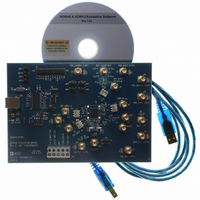
Manufacturer Part Number
AD9549/PCBZ
Description
BOARD EVALUATION FOR AD9549
Manufacturer
Analog Devices Inc
Datasheet
1.AD9549ABCPZ.pdf
(76 pages)
Specifications of AD9549/PCBZ
Main Purpose
Timing, Clock Generator
Embedded
No
Utilized Ic / Part
AD9549
Primary Attributes
2 Inputs, 2 Outputs, VCO
Secondary Attributes
CMOS, HSTL Output Logic, Graphical User Interface
Lead Free Status / RoHS Status
Lead free / RoHS Compliant


FREE-RUN (SINGLE-TONE) MODE (REGISTER 0x01A0 TO REGISTER 0x01AD)
Register 0x01A0 to Register 0x01A5—Reserved
Register 0x01A6—FTW0 (Frequency Tuning Word)
Table 60.
Bit
[7:0]
Register 0x01A7—FTW0 (Frequency Tuning Word) (Continued)
Table 61.
Bit
[15:8]
Register 0x01A8—FTW0 (Frequency Tuning Word) (Continued)
Table 62.
Bit
[23:16]
Register 0x01A9—FTW0 (Frequency Tuning Word) (Continued)
Table 63.
Bit
[31:24]
Register 0x01AA—FTW0 (Frequency Tuning Word) (Continued)
Table 64.
Bit
[39:32]
Register 0x01AB—FTW0 (Frequency Tuning Word) (Continued)
Table 65.
Bit
[47:40]
Bit Name
FTW0
Bit Name
FTW0
Bit Name
FTW0
Bit Name
FTW0
Bit Name
FTW0
Bit Name
FTW0
Description
FTW (frequency tuning word) for DDS when the loop is not closed (see Register 0x0100, Bit 0). Also used as
the initial frequency estimate when the estimator is disabled (see Register 0x0100, Bit 4) Note that the
power-up default is defined by the startup of Pin S1 to Pin S4 (see the Default DDS Output Frequency on
Power-Up section). Updates to the FTW results in an instantaneous frequency jump but no phase discontinuity.
Rev. D | Page 61 of 76
AD9549
Related parts for AD9549/PCBZ
Image
Part Number
Description
Manufacturer
Datasheet
Request
R


Part Number:
Description:
±1.7g Dual-Axis IMEMS Accelerometer Evaluation Board
Manufacturer:
Analog Devices Inc
Datasheet:

Part Number:
Description:
Inertial Sensor Evaluation System
Manufacturer:
Analog Devices Inc
Datasheet:
Part Number:
Description:
Manufacturer:
Analog Devices Inc
Datasheet:
Part Number:
Description:
Manufacturer:
Analog Devices Inc
Datasheet:
Part Number:
Description:
Manufacturer:
Analog Devices Inc
Datasheet:
Part Number:
Description:
Manufacturer:
Analog Devices Inc
Datasheet:
Part Number:
Description:
Manufacturer:
Analog Devices Inc
Datasheet:
Part Number:
Description:
Manufacturer:
Analog Devices Inc
Datasheet:
Part Number:
Description:
Manufacturer:
Analog Devices Inc
Datasheet:
Part Number:
Description:
Manufacturer:
Analog Devices Inc
Datasheet:
Part Number:
Description:
Manufacturer:
Analog Devices Inc
Datasheet:
Part Number:
Description:
Manufacturer:
Analog Devices Inc
Datasheet: