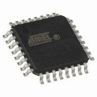
ATMEGA48-20AU Atmel, ATMEGA48-20AU Datasheet - Page 198

ATMEGA48-20AU
Manufacturer Part Number
ATMEGA48-20AU
Description
IC AVR MCU 4K 20MHZ 5V 32TQFP
Manufacturer
Atmel
Series
AVR® ATmegar
Specifications of ATMEGA48-20AU
Core Processor
AVR
Core Size
8-Bit
Speed
20MHz
Connectivity
I²C, SPI, UART/USART
Peripherals
Brown-out Detect/Reset, POR, PWM, WDT
Number Of I /o
23
Program Memory Size
4KB (2K x 16)
Program Memory Type
FLASH
Eeprom Size
256 x 8
Ram Size
512 x 8
Voltage - Supply (vcc/vdd)
2.7 V ~ 5.5 V
Data Converters
A/D 8x10b
Oscillator Type
Internal
Operating Temperature
-40°C ~ 85°C
Package / Case
32-TQFP, 32-VQFP
Processor Series
ATMEGA48x
Core
AVR8
Data Bus Width
8 bit
Data Ram Size
512 B
Interface Type
2-Wire/SPI/USART/Serial
Maximum Clock Frequency
20 MHz
Number Of Programmable I/os
23
Number Of Timers
3
Operating Supply Voltage
2.7 V to 5.5 V
Maximum Operating Temperature
+ 85 C
Mounting Style
SMD/SMT
3rd Party Development Tools
EWAVR, EWAVR-BL
Development Tools By Supplier
ATAVRDRAGON, ATSTK500, ATSTK600, ATAVRISP2, ATAVRONEKIT
Minimum Operating Temperature
- 40 C
On-chip Adc
8-ch x 10-bit
Cpu Family
ATmega
Device Core
AVR
Device Core Size
8b
Frequency (max)
20MHz
Total Internal Ram Size
512Byte
# I/os (max)
23
Number Of Timers - General Purpose
3
Operating Supply Voltage (typ)
3.3/5V
Operating Supply Voltage (max)
5.5V
Operating Supply Voltage (min)
2.7V
Instruction Set Architecture
RISC
Operating Temp Range
-40C to 85C
Operating Temperature Classification
Industrial
Mounting
Surface Mount
Pin Count
32
Package Type
TQFP
For Use With
ATSTK600-TQFP32 - STK600 SOCKET/ADAPTER 32-TQFPATSTK600-DIP40 - STK600 SOCKET/ADAPTER 40-PDIP770-1007 - ISP 4PORT ATMEL AVR MCU SPI/JTAG770-1005 - ISP 4PORT FOR ATMEL AVR MCU JTAG770-1004 - ISP 4PORT FOR ATMEL AVR MCU SPIATAVRDRAGON - KIT DRAGON 32KB FLASH MEM AVRATAVRISP2 - PROGRAMMER AVR IN SYSTEMATJTAGICE2 - AVR ON-CHIP D-BUG SYSTEM
Lead Free Status / RoHS Status
Lead free / RoHS Compliant
Available stocks
Company
Part Number
Manufacturer
Quantity
Price
Company:
Part Number:
ATMEGA48-20AU
Manufacturer:
ATMEL
Quantity:
6 460
Company:
Part Number:
ATMEGA48-20AU
Manufacturer:
Atmel
Quantity:
1 300
Company:
Part Number:
ATMEGA48-20AU
Manufacturer:
ATMEL
Quantity:
9 500
Part Number:
ATMEGA48-20AU
Manufacturer:
ATMEL/爱特梅尔
Quantity:
20 000
20. USART in SPI Mode
20.1
20.2
20.3
198
Features
Overview
Clock Generation
ATmega48/88/168
•
•
•
•
•
•
•
•
The Universal Synchronous and Asynchronous serial Receiver and Transmitter (USART) can be
set to a master SPI compliant mode of operation. Setting both UMSELn1:0 bits to one enables
the USART in Master SPI Mode (MSPIM) logic. In this mode of operation the SPI master control
logic takes direct control over the USART resources. These resources include the transmitter
and receiver shift register and buffers, and the baud rate generator. The parity generator and
checker, the data and clock recovery logic, and the RX and TX control logic is disabled. The
USART RX and TX control logic is replaced by a common SPI transfer control logic. However,
the pin control logic and interrupt generation logic is identical in both modes of operation.
The I/O register locations are the same in both modes. However, some of the functionality of the
control registers changes when using MSPIM.
The Clock Generation logic generates the base clock for the Transmitter and Receiver. For
USART MSPIM mode of operation only internal clock generation (that is, master operation) is
supported. The Data Direction Register for the XCKn pin (DDR_XCKn) must therefore be set to
one (that is, as output) for the USART in MSPIM to operate correctly. Preferably the DDR_XCKn
should be set up before the USART in MSPIM is enabled (that is, TXENn and RXENn bit set to
one).
The internal clock generation used in MSPIM mode is identical to the USART synchronous mas-
ter mode. The baud rate or UBRRn setting can therefore be calculated using the same
equations, see
Full Duplex, Three-wire Synchronous Data Transfer
Master Operation
Supports all four SPI Modes of Operation (Mode 0, 1, 2, and 3)
LSB First or MSB First Data Transfer (Configurable Data Order)
Queued Operation (Double Buffered)
High Resolution Baud Rate Generator
High Speed Operation (fXCKmax = fCK/2)
Flexible Interrupt Generation
Table
20-1:
2545S–AVR–07/10


