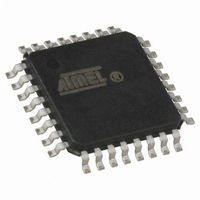
ATMEGA48-20AU Atmel, ATMEGA48-20AU Datasheet - Page 264

ATMEGA48-20AU
Manufacturer Part Number
ATMEGA48-20AU
Description
IC AVR MCU 4K 20MHZ 5V 32TQFP
Manufacturer
Atmel
Series
AVR® ATmegar
Specifications of ATMEGA48-20AU
Core Processor
AVR
Core Size
8-Bit
Speed
20MHz
Connectivity
I²C, SPI, UART/USART
Peripherals
Brown-out Detect/Reset, POR, PWM, WDT
Number Of I /o
23
Program Memory Size
4KB (2K x 16)
Program Memory Type
FLASH
Eeprom Size
256 x 8
Ram Size
512 x 8
Voltage - Supply (vcc/vdd)
2.7 V ~ 5.5 V
Data Converters
A/D 8x10b
Oscillator Type
Internal
Operating Temperature
-40°C ~ 85°C
Package / Case
32-TQFP, 32-VQFP
Processor Series
ATMEGA48x
Core
AVR8
Data Bus Width
8 bit
Data Ram Size
512 B
Interface Type
2-Wire/SPI/USART/Serial
Maximum Clock Frequency
20 MHz
Number Of Programmable I/os
23
Number Of Timers
3
Operating Supply Voltage
2.7 V to 5.5 V
Maximum Operating Temperature
+ 85 C
Mounting Style
SMD/SMT
3rd Party Development Tools
EWAVR, EWAVR-BL
Development Tools By Supplier
ATAVRDRAGON, ATSTK500, ATSTK600, ATAVRISP2, ATAVRONEKIT
Minimum Operating Temperature
- 40 C
On-chip Adc
8-ch x 10-bit
Cpu Family
ATmega
Device Core
AVR
Device Core Size
8b
Frequency (max)
20MHz
Total Internal Ram Size
512Byte
# I/os (max)
23
Number Of Timers - General Purpose
3
Operating Supply Voltage (typ)
3.3/5V
Operating Supply Voltage (max)
5.5V
Operating Supply Voltage (min)
2.7V
Instruction Set Architecture
RISC
Operating Temp Range
-40C to 85C
Operating Temperature Classification
Industrial
Mounting
Surface Mount
Pin Count
32
Package Type
TQFP
For Use With
ATSTK600-TQFP32 - STK600 SOCKET/ADAPTER 32-TQFPATSTK600-DIP40 - STK600 SOCKET/ADAPTER 40-PDIP770-1007 - ISP 4PORT ATMEL AVR MCU SPI/JTAG770-1005 - ISP 4PORT FOR ATMEL AVR MCU JTAG770-1004 - ISP 4PORT FOR ATMEL AVR MCU SPIATAVRDRAGON - KIT DRAGON 32KB FLASH MEM AVRATAVRISP2 - PROGRAMMER AVR IN SYSTEMATJTAGICE2 - AVR ON-CHIP D-BUG SYSTEM
Lead Free Status / RoHS Status
Lead free / RoHS Compliant
Available stocks
Company
Part Number
Manufacturer
Quantity
Price
Company:
Part Number:
ATMEGA48-20AU
Manufacturer:
ATMEL
Quantity:
6 460
Company:
Part Number:
ATMEGA48-20AU
Manufacturer:
Atmel
Quantity:
1 300
Company:
Part Number:
ATMEGA48-20AU
Manufacturer:
ATMEL
Quantity:
9 500
Part Number:
ATMEGA48-20AU
Manufacturer:
ATMEL/爱特梅尔
Quantity:
20 000
25.2.4
25.2.5
264
ATmega48/88/168
Programming Time for Flash when Using SPM
Simple Assembly Code Example for a Boot Loader
A Flash program corruption can be caused by two situations when the voltage is too low. First, a
regular write sequence to the Flash requires a minimum voltage to operate correctly. Secondly,
the CPU itself can execute instructions incorrectly, if the supply voltage for executing instructions
is too low.
Flash corruption can easily be avoided by following these design recommendations (one is
sufficient):
1. Keep the AVR RESET active (low) during periods of insufficient power supply voltage.
2. Keep the AVR core in Power-down sleep mode during periods of low V
The calibrated RC Oscillator is used to time Flash accesses.
gramming time for Flash accesses from the CPU.
Table 25-1.
Note:
Note that the RWWSB bit will always be read as zero in ATmega48. Nevertheless, it is recom-
mended to check this bit as shown in the code example, to ensure compatibility with devices
supporting Read-While-Write.
Flash write (Page Erase, Page Write, and
write Lock bits by SPM)
This can be done by enabling the internal Brown-out Detector (BOD) if the operating volt-
age matches the detection level. If not, an external low V
used. If a reset occurs while a write operation is in progress, the write operation will be
completed provided that the power supply voltage is sufficient.
vent the CPU from attempting to decode and execute instructions, effectively protecting
the SPMCSR Register and thus the Flash from unintentional writes.
.equ PAGESIZEB = PAGESIZE*2
.org SMALLBOOTSTART
Write_page:
;-the routine writes one page of data from RAM to Flash
; the first data location in RAM is pointed to by the Y pointer
; the first data location in Flash is pointed to by the Z-pointer
;-error handling is not included
;-the routine must be placed inside the Boot space
; (at least the Do_spm sub routine). Only code inside NRWW section can
; be read during Self-Programming (Page Erase and Page Write).
;-registers used: r0, r1, temp1 (r16), temp2 (r17), looplo (r24),
; loophi (r25), spmcrval (r20)
; storing and restoring of registers is not included in the routine
; register usage can be optimized at the expense of code size
;-It is assumed that either the interrupt table is moved to the Boot
; loader section or that the interrupts are disabled.
; Page Erase
ldi
rcallDo_spm
; re-enable the RWW section
ldi
1. Minimum and maximum programming time is per individual operation.
spmcrval, (1<<PGERS) | (1<<SELFPRGEN)
spmcrval, (1<<RWWSRE) | (1<<SELFPRGEN)
SPM Programming Time
Symbol
(1)
;PAGESIZEB is page size in BYTES, not words
Min Programming Time
3.7 ms
CC
Table 26-5
reset protection circuit can be
Max Programming Time
shows the typical pro-
CC
. This will pre-
4.5 ms
2545S–AVR–07/10


