P87C660X2BBD,157 NXP Semiconductors, P87C660X2BBD,157 Datasheet - Page 76
P87C660X2BBD,157
Manufacturer Part Number
P87C660X2BBD,157
Description
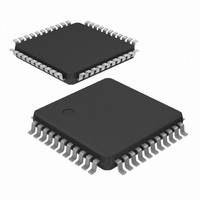
IC 80C51 MCU 16K OTP 44-LQFP
Manufacturer
NXP Semiconductors
Series
87Cr
Datasheet
1.P87C660X2BBD157.pdf
(102 pages)
Specifications of P87C660X2BBD,157
Core Processor
8051
Core Size
8-Bit
Speed
33MHz
Connectivity
EBI/EMI, I²C, UART/USART
Peripherals
POR, PWM, WDT
Number Of I /o
32
Program Memory Size
16KB (16K x 8)
Program Memory Type
OTP
Ram Size
512 x 8
Voltage - Supply (vcc/vdd)
2.7 V ~ 5.5 V
Oscillator Type
Internal
Operating Temperature
0°C ~ 70°C
Package / Case
44-LQFP
Processor Series
P87C6x
Core
80C51
Data Bus Width
8 bit
Data Ram Size
512 B
Interface Type
I2C, UART
Maximum Clock Frequency
16 MHz, 33 MHz
Number Of Programmable I/os
32
Number Of Timers
3
Operating Supply Voltage
2.7 V to 5.5 V
Maximum Operating Temperature
+ 70 C
Mounting Style
SMD/SMT
3rd Party Development Tools
PK51, CA51, A51, ULINK2
Minimum Operating Temperature
0 C
Lead Free Status / RoHS Status
Lead free / RoHS Compliant
Eeprom Size
-
Data Converters
-
Lead Free Status / Rohs Status
Details
Other names
568-3204
935273061157
P87C660X2BBD
935273061157
P87C660X2BBD
Available stocks
Company
Part Number
Manufacturer
Quantity
Price
Company:

Part Number:
P87C660X2BBD,157
Manufacturer:
NXP Semiconductors
Quantity:
10 000


Philips Semiconductors
2003 Oct 02
80C51 8-bit microcontroller family
RAM, low voltage (2.7 to 5.5 V), low power, high speed (30/33
MHz), two 400KB I
NOTE:
*User software should not write 1s to reserved bits. These bits may be used in future 8051 family products to invoke new features. In that case, the reset or inactive value
of the new bit will be 0, and its active value will be 1. The value read from a reserved bit is indeterminate.
AUXR
Symbol
AO
EXTRAM
FME
SRD
—
Address = 8EH
Not Bit Addressable
Bit:
Function
Disable/Enable ALE
AO
0
1
Internal/External RAM access using MOVX @Ri/@DPTR
EXTRAM
0
1
Fast Mode Enable, switches between the Standard and the Fast data-transfer mode for the SIO1 I
one-time set bit, cleared by chip-reset only)
FME
0
1
Slew-Rate control-circuit Disable, switches between the minimum and the maximum slew-rate of the SCL1 and SDA1 pins
of the SIO2 I
SRD
0
1
Not implemented, reserved for future use*.
100
2
C interfaces
—
7
Figure 49. Internal and External Data Memory Address Space with EXTRAM = 0
2
256 BYTES
C serial port.
ERAM
Operating Mode
ALE is emitted at a constant rate of
in 6-clock mode).
ALE is active only during off-chip memory access.
Operating Mode
Internal ERAM access using MOVX @Ri/@DPTR.
External data memory access.
Operating Mode
100 Kbit/s Standard mode selected.
400 kbit/s Fast mode selected.
Operating Mode
Minimum output slew-rate.
Maximum output slew-rate.
—
6
16 KB OTP/ROM, 512B
FF
80
00
SRD
5
Figure 48. AUXR: Auxiliary Register
INTERNAL RAM
INTERNAL RAM
128 BYTES
128 BYTES
LOWER
UPPER
—
4
76
1
FME
/
FF
6
80
00
3
the oscillator frequency (12-clock mode;
FUNCTION
REGISTER
SPECIAL
—
2
EXTRAM
1
3FFF
0000
AO
EXTERNAL
P8xC660X2/661X2
0
MEMORY
DATA
Reset Value = xx0x 0x00B
1
/
2
3
C serial port (a
f
OSC
SU01750
Product data
SU01749
Related parts for P87C660X2BBD,157
Image
Part Number
Description
Manufacturer
Datasheet
Request
R

Part Number:
Description:
80C51 8-bit microcontroller family
Manufacturer:
PHILIPS [NXP Semiconductors]
Datasheet:

Part Number:
Description:
NXP Semiconductors designed the LPC2420/2460 microcontroller around a 16-bit/32-bitARM7TDMI-S CPU core with real-time debug interfaces that include both JTAG andembedded trace
Manufacturer:
NXP Semiconductors
Datasheet:

Part Number:
Description:
NXP Semiconductors designed the LPC2458 microcontroller around a 16-bit/32-bitARM7TDMI-S CPU core with real-time debug interfaces that include both JTAG andembedded trace
Manufacturer:
NXP Semiconductors
Datasheet:
Part Number:
Description:
NXP Semiconductors designed the LPC2468 microcontroller around a 16-bit/32-bitARM7TDMI-S CPU core with real-time debug interfaces that include both JTAG andembedded trace
Manufacturer:
NXP Semiconductors
Datasheet:
Part Number:
Description:
NXP Semiconductors designed the LPC2470 microcontroller, powered by theARM7TDMI-S core, to be a highly integrated microcontroller for a wide range ofapplications that require advanced communications and high quality graphic displays
Manufacturer:
NXP Semiconductors
Datasheet:
Part Number:
Description:
NXP Semiconductors designed the LPC2478 microcontroller, powered by theARM7TDMI-S core, to be a highly integrated microcontroller for a wide range ofapplications that require advanced communications and high quality graphic displays
Manufacturer:
NXP Semiconductors
Datasheet:
Part Number:
Description:
The Philips Semiconductors XA (eXtended Architecture) family of 16-bit single-chip microcontrollers is powerful enough to easily handle the requirements of high performance embedded applications, yet inexpensive enough to compete in the market for hi
Manufacturer:
NXP Semiconductors
Datasheet:
Part Number:
Description:
The XA-S3 device is a member of Philips Semiconductors? XA(eXtended Architecture) family of high performance 16-bitsingle-chip microcontrollers
Manufacturer:
NXP Semiconductors
Datasheet:

Part Number:
Description:
The NXP BlueStreak LH75401/LH75411 family consists of two low-cost 16/32-bit System-on-Chip (SoC) devices
Manufacturer:
NXP Semiconductors
Datasheet:
Part Number:
Description:
The NXP LPC3130/3131 combine an 180 MHz ARM926EJ-S CPU core, high-speed USB2
Manufacturer:
NXP Semiconductors
Datasheet:
Part Number:
Description:
The NXP LPC3141 combine a 270 MHz ARM926EJ-S CPU core, High-speed USB 2
Manufacturer:
NXP Semiconductors
Part Number:
Description:
The NXP LPC3143 combine a 270 MHz ARM926EJ-S CPU core, High-speed USB 2
Manufacturer:
NXP Semiconductors

Part Number:
Description:
The NXP LPC3152 combines an 180 MHz ARM926EJ-S CPU core, High-speed USB 2
Manufacturer:
NXP Semiconductors
Part Number:
Description:
The NXP LPC3154 combines an 180 MHz ARM926EJ-S CPU core, High-speed USB 2
Manufacturer:
NXP Semiconductors