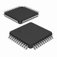
P87C660X2BBD,157 NXP Semiconductors, P87C660X2BBD,157 Datasheet - Page 93

P87C660X2BBD,157
Manufacturer Part Number
P87C660X2BBD,157
Description
IC 80C51 MCU 16K OTP 44-LQFP
Manufacturer
NXP Semiconductors
Series
87Cr
Datasheet
1.P87C660X2BBD157.pdf
(102 pages)
Specifications of P87C660X2BBD,157
Core Processor
8051
Core Size
8-Bit
Speed
33MHz
Connectivity
EBI/EMI, I²C, UART/USART
Peripherals
POR, PWM, WDT
Number Of I /o
32
Program Memory Size
16KB (16K x 8)
Program Memory Type
OTP
Ram Size
512 x 8
Voltage - Supply (vcc/vdd)
2.7 V ~ 5.5 V
Oscillator Type
Internal
Operating Temperature
0°C ~ 70°C
Package / Case
44-LQFP
Processor Series
P87C6x
Core
80C51
Data Bus Width
8 bit
Data Ram Size
512 B
Interface Type
I2C, UART
Maximum Clock Frequency
16 MHz, 33 MHz
Number Of Programmable I/os
32
Number Of Timers
3
Operating Supply Voltage
2.7 V to 5.5 V
Maximum Operating Temperature
+ 70 C
Mounting Style
SMD/SMT
3rd Party Development Tools
PK51, CA51, A51, ULINK2
Minimum Operating Temperature
0 C
Lead Free Status / RoHS Status
Lead free / RoHS Compliant
Eeprom Size
-
Data Converters
-
Lead Free Status / Rohs Status
Details
Other names
568-3204
935273061157
P87C660X2BBD
935273061157
P87C660X2BBD
Available stocks
Company
Part Number
Manufacturer
Quantity
Price
Company:
Part Number:
P87C660X2BBD,157
Manufacturer:
NXP Semiconductors
Quantity:
10 000
Philips Semiconductors
EPROM CHARACTERISTICS
All these devices can be programmed by using a modified Improved
Quick-Pulse Programming
in the value used for V
width and number of the ALE/PROG pulses.
The family contains two signature bytes that can be read and used
by an EPROM programming system to identify the device. The
signature bytes identify the device as being manufactured by
Philips.
Table 17 shows the logic levels for reading the signature byte, and
for programming the program memory, the encryption table, and the
security bits. The circuit configuration and waveforms for quick-pulse
programming are shown in Figures 64 and 65. Figure 66 shows the
circuit configuration for normal program memory verification.
Quick-Pulse Programming
The setup for microcontroller quick-pulse programming is shown in
Figure 64. Note that the device is running with a 4 to 6MHz
oscillator. The reason the oscillator needs to be running is that the
device is executing internal address and program data transfers.
The address of the EPROM location to be programmed is applied to
ports 1 and 2, as shown in Figure 64. The code byte to be
programmed into that location is applied to port 0. RST, PSEN and
pins of ports 2 and 3 specified in Table 17 are held at the ‘Program
Code Data’ levels indicated in Table 17. The ALE/PROG is pulsed
LOW 5 times as shown in Figure 65.
To program the encryption table, repeat the 5 pulse programming
sequence for addresses 0 through 1FH, using the ‘Pgm Encryption
Table’ levels. Do not forget that after the encryption table is
programmed, verification cycles will produce only encrypted data.
To program the security bits, repeat the 5 pulse programming
sequence using the ‘Pgm Security Bit’ levels. After one security bit is
programmed, further programming of the code memory and
encryption table is disabled. However, the other security bits can still
be programmed.
Note that the EA/V
maximum specified V
glitch above that voltage can cause permanent damage to the
device. The V
and overshoot.
2003 Oct 02
Trademark phrase of Intel Corporation.
80C51 8-bit microcontroller family
RAM, low voltage (2.7 to 5.5 V), low power, high speed (30/33
MHz), two 400KB I
PP
source should be well regulated and free of glitches
PP
PP
pin must not be allowed to go above the
PP
2
level for any amount of time. Even a narrow
C interfaces
(programming supply voltage) and in the
algorithm. It differs from older methods
16 KB OTP/ROM, 512B
93
Program Verification
If security bits 2 and 3 have not been programmed, the on-chip
program memory can be read out for program verification. The
address of the program memory locations to be read is applied to
ports 1 and 2 as shown in Figure 66. The other pins are held at the
‘Verify Code Data’ levels indicated in Table 17. The contents of the
address location will be emitted on port 0. External pull-ups are
required on port 0 for this operation.
If the 64 byte encryption table has been programmed, the data
presented at port 0 will be the exclusive NOR of the program byte
with one of the encryption bytes. The user will have to know the
encryption table contents in order to correctly decode the verification
data. The encryption table itself cannot be read out.
Reading the Signature Bytes
The signature bytes are read by the same procedure as a normal
verification of locations 030H and 031H, except that P3.6 and P3.7
need to be pulled to a logic LOW. The values are:
(030H) = 15H indicates manufactured by Philips
(031H) = C9H indicates P8xC66xX2
(060H) = 01H (660)
Program/Verify Algorithms
Any algorithm in agreement with the conditions listed in Table 17,
and which satisfies the timing specifications, is suitable.
Security Bits
With none of the security bits programmed the code in the program
memory can be verified. If the encryption table is programmed, the
code will be encrypted when verified. When only security bit 1 (see
Table 18) is programmed, MOVC instructions executed from
external program memory are disabled from fetching code bytes
from the internal memory, EA is latched on Reset and all further
programming of the EPROM is disabled. When security bits 1 and 2
are programmed, in addition to the above, verify mode is disabled.
When all three security bits are programmed, all of the conditions
above apply and all external program memory execution is disabled.
Encryption Array
64 bytes of encryption array are initially unprogrammed (all 1s).
02H (661)
P8xC660X2/661X2
Product data


