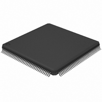
LPC2210FBD144/01,5 NXP Semiconductors, LPC2210FBD144/01,5 Datasheet - Page 23

LPC2210FBD144/01,5
Manufacturer Part Number
LPC2210FBD144/01,5
Description
IC ARM7 MCU 16KRAM W/ADC 144LQFP
Manufacturer
NXP Semiconductors
Series
LPC2200r
Datasheet
1.LPC2210FBD144015.pdf
(50 pages)
Specifications of LPC2210FBD144/01,5
Program Memory Type
ROMless
Package / Case
144-LQFP
Core Processor
ARM7
Core Size
16/32-Bit
Speed
60MHz
Connectivity
EBI/EMI, I²C, Microwire, SPI, SSI, SSP, UART/USART
Peripherals
POR, PWM, WDT
Number Of I /o
76
Ram Size
16K x 8
Voltage - Supply (vcc/vdd)
1.65 V ~ 3.6 V
Data Converters
A/D 8x10b
Oscillator Type
Internal
Operating Temperature
-40°C ~ 85°C
Processor Series
LPC22
Core
ARM7TDMI-S
Data Bus Width
16 bit, 32 bit
Data Ram Size
16 KB
Interface Type
I2C/SPI/SSP/UART
Maximum Clock Frequency
60 MHz
Number Of Programmable I/os
76
Number Of Timers
2
Operating Supply Voltage
3.3 V
Maximum Operating Temperature
+ 85 C
Mounting Style
SMD/SMT
3rd Party Development Tools
MDK-ARM, RL-ARM, ULINK2
Minimum Operating Temperature
- 40 C
On-chip Adc
8-ch x 10-bit
Lead Free Status / RoHS Status
Lead free / RoHS Compliant
For Use With
OM10091 - KIT DEV PHYCORE-ARM7/LPC2220622-1005 - USB IN-CIRCUIT PROG ARM7 LPC2K568-1757 - BOARD EVAL FOR LPC220X ARM MCU
Eeprom Size
-
Program Memory Size
-
Lead Free Status / Rohs Status
Lead free / RoHS Compliant
Other names
568-4012
935282078551
LPC2210FBD144/01-S
935282078551
LPC2210FBD144/01-S
Available stocks
Company
Part Number
Manufacturer
Quantity
Price
Company:
Part Number:
LPC2210FBD144/01,5
Manufacturer:
NXP Semiconductors
Quantity:
10 000
NXP Semiconductors
Table 9.
LPC2210_2220_6
Product data sheet
PINSEL2 bits
23
24
27:25
31:28
Pin function select register 2 (PINSEL2 - 0xE002 C014)
6.10.1 Features
6.11.1 Features
6.10 General purpose parallel I/O
6.11 10-bit ADC
6.9 External memory controller
Description
Controls whether P3.0/A0 is a port pin (0) or an address line (1).
Controls whether P3.1/A1 is a port pin (0) or an address line (1).
Controls the number of pins among P3.23/A23/XCLK and P3[22:2]/A2[22:2] that
are address lines:
000 = None
001 = A3 to A2 are address
lines.
010 = A5 to A2 are address
lines.
011 = A7 to A2 are address
lines.
reserved
The external static memory controller is a module which provides an interface between
the system bus and external (off-chip) memory devices. It provides support for up to four
independently configurable memory banks (16 MB each with byte lane enable control)
simultaneously. Each memory bank is capable of supporting SRAM, ROM, flash EPROM,
burst ROM memory, or some external I/O devices.
Each memory bank may be 8-bit, 16-bit, or 32-bit wide.
Device pins that are not connected to a specific peripheral function are controlled by the
GPIO registers. Pins may be dynamically configured as inputs or outputs. Separate
registers allow setting or clearing any number of outputs simultaneously. The value of the
output register may be read back, as well as the current state of the port pins.
The LPC2210/2220 each contain a single 10-bit successive approximation ADC with eight
multiplexed channels.
•
•
•
•
•
•
Direction control of individual bits.
Separate control of output set and clear.
All I/O default to inputs after reset.
Measurement range of 0 V to 3 V.
Capable of performing more than 400000 10-bit samples per second.
Burst conversion mode for single or multiple inputs.
Rev. 06 — 11 December 2008
100 = A11 to A2 are address lines.
101 = A15 to A2 are address lines.
110 = A19 to A2 are address lines.
111 = A23 to A2 are address lines.
…continued
16/32-bit ARM microcontrollers
LPC2210/2220
Reset value
1 if BOOT1:0 = 00
at RESET = 0,
0 otherwise
BOOT1 during
reset
000 if
BOOT1:0 = 11 at
reset, 111
otherwise
© NXP B.V. 2008. All rights reserved.
23 of 50


