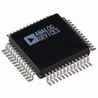
ADUC834BSZ Analog Devices Inc, ADUC834BSZ Datasheet - Page 64

ADUC834BSZ
Manufacturer Part Number
ADUC834BSZ
Description
IC ADC DUAL16/24BIT W/MCU 52MQFP
Manufacturer
Analog Devices Inc
Series
MicroConverter® ADuC8xxr
Specifications of ADUC834BSZ
Core Size
8-Bit
Program Memory Size
62KB (62K x 8)
Oscillator Type
Internal
Core Processor
8052
Speed
12.58MHz
Connectivity
EBI/EMI, I²C, SPI, UART/USART
Peripherals
POR, PSM, PWM, Temp Sensor, WDT
Number Of I /o
34
Program Memory Type
FLASH
Eeprom Size
4K x 8
Ram Size
2.25K x 8
Voltage - Supply (vcc/vdd)
2.7 V ~ 5.25 V
Data Converters
A/D 3x16b, 4x24b; D/A 1x12b
Operating Temperature
-40°C ~ 125°C
Package / Case
52-MQFP, 52-PQFP
Controller Family/series
(8052) ADUC
No. Of I/o's
26
Eeprom Memory Size
62KB
Ram Memory Size
2KB
Cpu Speed
12.58MHz
Package
52MQFP
Device Core
8052
Family Name
ADuC8xx
Maximum Speed
12.58 MHz
Operating Supply Voltage
3.3|5 V
Data Bus Width
8 Bit
Number Of Programmable I/os
26
Interface Type
I2C/SPI/UART
On-chip Adc
4-chx16-bit|4-chx24-bit
On-chip Dac
1-chx12-bit
Number Of Timers
3
Lead Free Status / RoHS Status
Lead free / RoHS Compliant
Available stocks
Company
Part Number
Manufacturer
Quantity
Price
Company:
Part Number:
ADUC834BSZ
Manufacturer:
TOSHIBA
Quantity:
1 200
Company:
Part Number:
ADUC834BSZ
Manufacturer:
Analog Devices Inc
Quantity:
10 000
Part Number:
ADUC834BSZ
Manufacturer:
ADI/亚德诺
Quantity:
20 000
ADuC834
Power Supplies
The ADuC834’s operational power supply voltage range is
2.7 V to 5.25 V. Although the guaranteed data sheet specifica-
tions are given only for power supplies within 2.7 V to 3.6 V or
5% of the nominal 5 V level, the chip will function equally well
at any power supply level between 2.7 V and 5.25 V.
Separate analog and digital power supply pins (AV
respectively) allow AV
tal signals often present on the system DV
the part can also operate with split supplies; that is, using differ-
ent voltage supply levels for each supply. For example, this
means that the system can be designed to operate with a DV
voltage level of 3 V while the AV
versa if required. A typical split supply configuration is shown in
Figure 61.
As an alternative to providing two separate power supplies,
AV
ferrite bead between it and DV
separately to ground. An example of this configuration is shown
in Figure 62. In this configuration, other analog circuitry (such
as op amps, voltage reference, and so on) can be powered from
the AV
DD
Figure 62. External Single Supply Connections
can be kept quiet by placing a small series resistor and/or
DD
Figure 61. External Dual Supply Connections
DIGITAL SUPPLY
0.1 F
supply line as well.
0.1 F
+
–
+
–
DIGITAL SUPPLY
10 F
DD
10 F
to be kept relatively free of noisy digi-
20
34
48
21
35
47
47
20
34
48
21
35
DV
DGND
DV
DGND
BEAD
DD
DD
DD
ADuC834
ADuC834
DD
, and then decoupling AV
level can be at 5 V, or vice-
1.6
AGND
AGND
AV
AV
ANALOG SUPPLY
DD
DD
10 F
DD
5
6
5
6
line. In this mode,
10 F
0.1 F
0.1 F
DD
+
–
and DV
DD
DD
DD
–64–
Notice that in both Figure 61 and Figure 62 a large value (10 F)
reservoir capacitor sits on DV
sits on AV
located at each V
practice, be sure to include all of these capacitors and ensure
the smaller capacitors are closest to each V
lengths as short as possible. Connect the ground terminal of
each of these capacitors directly to the underlying ground plane.
Finally, it should also be noticed that, at all times, the analog
and digital ground pins on the ADuC834 should be referenced
to the same system ground reference point.
Power-On Reset Operation
An internal POR (Power-On Reset) is implemented on the
ADuC834. For DV
the ADuC834 in reset. As DV
timer will time out for typically 128 ms before the part is
released from reset. The user must ensure that the power supply
has reached a stable 2.7 V minimum level by this time. Likewise
on power-down, the internal POR will hold the ADuC834 in
reset until the power supply has dropped below 1 V. Figure 63
illustrates the operation of the internal POR in detail.
Power Consumption
The DV
normal, idle, and power-down modes. The AV
current is specified with the analog peripherals disabled. The
normal mode power consumption represents the current drawn
from DV
(watchdog timer, power supply monitor, and so on) consume
negligible current and are therefore lumped in with the normal
operating current here. Of course, the user must add any cur-
rents sourced by the parallel and serial I/O pins, and those
sourced by the DAC in order to determine the total current
needed at the ADuC834’s DV
current drawn from the DV
mately 5 mA during Flash/EE erase and program cycles.
DV
CORE RESET
INTERNAL
DD
Figure 63. Internal Power-on-Reset Operation
2.45V TYP
DD
1.0V TYP
DD
DD
power supply current consumption is specified in
by the digital core. The other on-chip peripherals
. Also, local decoupling capacitors (0.1 F) are
DD
DD
pin of the chip. As per standard design
128ms TYP
below 2.45 V, the internal POR will hold
DD
DD
DD
DD
supply will increase by approxi-
and a separate 10 F capacitor
rises above 2.45 V, an internal
and AV
128ms TYP
DD
supply pins. Also,
DD
DD
pin with lead
power supply
1.0V TYP
REV. A


