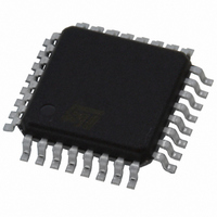
ST72F324BK4T3 STMicroelectronics, ST72F324BK4T3 Datasheet - Page 99

ST72F324BK4T3
Manufacturer Part Number
ST72F324BK4T3
Description
IC MCU 8BIT 16K FLASH 32-TQFP
Manufacturer
STMicroelectronics
Series
ST7r
Datasheet
1.ST72F324BJ2T6.pdf
(198 pages)
Specifications of ST72F324BK4T3
Core Processor
ST7
Core Size
8-Bit
Speed
8MHz
Connectivity
SCI, SPI
Peripherals
LVD, POR, PWM, WDT
Number Of I /o
24
Program Memory Size
16KB (16K x 8)
Program Memory Type
FLASH
Ram Size
512 x 8
Voltage - Supply (vcc/vdd)
3.8 V ~ 5.5 V
Data Converters
A/D 12x10b
Oscillator Type
Internal
Operating Temperature
-40°C ~ 125°C
Package / Case
32-TQFP, 32-VQFP
Processor Series
ST72F3x
Core
ST7
Data Bus Width
8 bit
Data Ram Size
512 B
Interface Type
SCI, SPI
Maximum Clock Frequency
8 MHz
Number Of Programmable I/os
32
Number Of Timers
3
Maximum Operating Temperature
+ 125 C
Mounting Style
SMD/SMT
Development Tools By Supplier
ST7232X-EVAL, ST7MDT20-DVP3, ST7MDT20J-EMU3, STX-RLINK
Minimum Operating Temperature
- 40 C
On-chip Adc
10 bit, 12 Channel
A/d Bit Size
10 bit
A/d Channels Available
12
Height
1.4 mm
Length
7 mm
Supply Voltage (max)
5.5 V
Supply Voltage (min)
3.8 V
Width
7 mm
For Use With
497-6421 - BOARD EVAL DGTL BATT CHGR DESIGN497-5046 - KIT TOOL FOR ST7/UPSD/STR7 MCU
Lead Free Status / RoHS Status
Lead free / RoHS Compliant
Eeprom Size
-
Lead Free Status / Rohs Status
Details
Other names
497-8241
ST72F324BK4T3
ST72F324BK4T3
Available stocks
Company
Part Number
Manufacturer
Quantity
Price
Company:
Part Number:
ST72F324BK4T3
Manufacturer:
STMicroelectronics
Quantity:
10 000
Company:
Part Number:
ST72F324BK4T3TR
Manufacturer:
STMicroelectronics
Quantity:
10 000
ST72324B-Auto
The MOSI pins are connected together and the MISO pins are connected together. In this
way data is transferred serially between master and slave (most significant bit first).
The communication is always initiated by the master. When the master device transmits
data to a slave device via MOSI pin, the slave device responds by sending data to the
master device via the MISO pin. This implies full duplex communication with both data out
and data in synchronized with the same clock signal (which is provided by the master device
via the SCK pin).
To use a single data line, the MISO and MOSI pins must be connected at each node (in this
case only simplex communication is possible).
Four possible data/clock timing relationships may be chosen (see
slave must be programmed with the same timing mode.
Figure 49. Single master/single slave application
Slave Select management
As an alternative to using the SS pin to control the Slave Select signal, the application can
choose to manage the Slave Select signal by software. This is configured by the SSM bit in
the SPICSR register (see
In software management, the external SS pin is free for other application uses and the
internal SS signal level is driven by writing to the SSI bit in the SPICSR register.
In Master mode:
●
Depending on the data/clock timing relationship, there are two cases in Slave mode (see
Figure
If CPHA = 1 (data latched on second clock edge):
●
If CPHA = 0 (data latched on first clock edge):
●
SS internal must be held high continuously
SS internal must be held low during the entire transmission. This implies that in single
slave applications the SS pin either can be tied to V
managing the SS function by software (SSM = 1 and SSI = 0 in the in the SPICSR
register)
SS internal must be held low during byte transmission and pulled high between each
byte to allow the slave to write to the shift register. If SS is not pulled high, a Write
50):
MSB
generator
clock
8-bit Shift Register
SPI
Master
Figure
LSB
Doc ID13466 Rev 4
51).
MOSI
SCK
SS
MISO
+5V
MISO
MOSI
SCK
SS
SS
, or made free for standard I/O by
MSB
Not used if SS is managed
by software
Figure
8-bit Shift Register
On-chip peripherals
Slave
52) but master and
LSB
99/198


