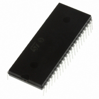
ST72F324BJ6B6 STMicroelectronics, ST72F324BJ6B6 Datasheet - Page 77

ST72F324BJ6B6
Manufacturer Part Number
ST72F324BJ6B6
Description
MCU 8BIT 32KB FLASH/ROM 42-SDIP
Manufacturer
STMicroelectronics
Series
ST7r
Datasheet
1.ST72F324BJ6B6.pdf
(193 pages)
Specifications of ST72F324BJ6B6
Core Processor
ST7
Core Size
8-Bit
Speed
8MHz
Connectivity
SCI, SPI
Peripherals
LVD, POR, PWM, WDT
Number Of I /o
32
Program Memory Size
32KB (32K x 8)
Program Memory Type
FLASH
Ram Size
1K x 8
Voltage - Supply (vcc/vdd)
3.8 V ~ 5.5 V
Data Converters
A/D 12x10b
Oscillator Type
Internal
Operating Temperature
-40°C ~ 85°C
Package / Case
42-SDIP (0.600", 15.24mm)
Controller Family/series
ST7
No. Of I/o's
32
Ram Memory Size
1KB
Cpu Speed
8MHz
No. Of Timers
2
Embedded Interface Type
SCI, SPI
No. Of Pwm Channels
3
Processor Series
ST72F3x
Core
ST7
Data Bus Width
8 bit
Data Ram Size
1 KB
Interface Type
SCI, SPI
Maximum Clock Frequency
8 MHz
Number Of Programmable I/os
32
Number Of Timers
3
Maximum Operating Temperature
+ 85 C
Mounting Style
Through Hole
Development Tools By Supplier
ST7232X-EVAL, ST7MDT20-DVP3, ST7MDT20J-EMU3, STX-RLINK
Minimum Operating Temperature
- 40 C
On-chip Adc
10 bit, 12 Channel
For Use With
497-6421 - BOARD EVAL DGTL BATT CHGR DESIGN497-5046 - KIT TOOL FOR ST7/UPSD/STR7 MCU
Lead Free Status / RoHS Status
Lead free / RoHS Compliant
Eeprom Size
-
Lead Free Status / Rohs Status
Details
Other names
497-5589-5
- Current page: 77 of 193
- Download datasheet (3Mb)
ST72324Bxx
Note:
16-bit read sequence
The 16-bit read sequence (from either the Counter register or the Alternate Counter
register) is illustrated in the following
Figure 37.
The user must first read the MSB, afterwhich the LSB value is automatically buffered.
This buffered value remains unchanged until the 16-bit read sequence is completed, even if
the user reads the MSB several times.
After a complete reading sequence, if only the CLR register or ACLR register are read, they
return the LSB of the count value at the time of the read.
Whatever the timer mode used (input capture, output compare, one pulse mode or PWM
mode) an overflow occurs when the counter rolls over from FFFFh to 0000h then:
●
●
If one of these conditions is false, the interrupt remains pending to be issued as soon as
they are both true.
Clearing the overflow interrupt request is done in two steps:
1.
2.
The TOF bit is not cleared by access to the ACLR register. The advantage of accessing the
ACLR register rather than the CLR register is that it allows simultaneous use of the overflow
function and reading the free running counter at random times (for example, to measure
elapsed time) without the risk of clearing the TOF bit erroneously.
The timer is not affected by Wait mode.
In Halt mode, the counter stops counting until the mode is exited. Counting then resumes
from the previous count (MCU awakened by an interrupt) or from the reset count (MCU
awakened by a reset).
The TOF bit of the SR register is set.
A timer interrupt is generated if:
–
–
Reading the SR register while the TOF bit is set.
An access (read or write) to the CLR register.
TOIE bit of the CR1 register is set and
I bit of the CC register is cleared.
16-bit read sequence
At t0 +Δt
Beginning of the sequence
At t0
Sequence completed
Read
instructions
Read
Figure
Other
MSB
LSB
37.
Returns the buffered
LSB value at t0
LSB is buffered
On-chip peripherals
77/193
Related parts for ST72F324BJ6B6
Image
Part Number
Description
Manufacturer
Datasheet
Request
R

Part Number:
Description:
STMicroelectronics [RIPPLE-CARRY BINARY COUNTER/DIVIDERS]
Manufacturer:
STMicroelectronics
Datasheet:

Part Number:
Description:
STMicroelectronics [LIQUID-CRYSTAL DISPLAY DRIVERS]
Manufacturer:
STMicroelectronics
Datasheet:

Part Number:
Description:
BOARD EVAL FOR MEMS SENSORS
Manufacturer:
STMicroelectronics
Datasheet:

Part Number:
Description:
NPN TRANSISTOR POWER MODULE
Manufacturer:
STMicroelectronics
Datasheet:

Part Number:
Description:
TURBOSWITCH ULTRA-FAST HIGH VOLTAGE DIODE
Manufacturer:
STMicroelectronics
Datasheet:

Part Number:
Description:
Manufacturer:
STMicroelectronics
Datasheet:

Part Number:
Description:
DIODE / SCR MODULE
Manufacturer:
STMicroelectronics
Datasheet:

Part Number:
Description:
DIODE / SCR MODULE
Manufacturer:
STMicroelectronics
Datasheet:

Part Number:
Description:
Search -----> STE16N100
Manufacturer:
STMicroelectronics
Datasheet:

Part Number:
Description:
Search ---> STE53NA50
Manufacturer:
STMicroelectronics
Datasheet:

Part Number:
Description:
NPN Transistor Power Module
Manufacturer:
STMicroelectronics
Datasheet:


