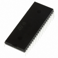
ST72F324BJ6B6 STMicroelectronics, ST72F324BJ6B6 Datasheet - Page 79

ST72F324BJ6B6
Manufacturer Part Number
ST72F324BJ6B6
Description
MCU 8BIT 32KB FLASH/ROM 42-SDIP
Manufacturer
STMicroelectronics
Series
ST7r
Datasheet
1.ST72F324BJ6B6.pdf
(193 pages)
Specifications of ST72F324BJ6B6
Core Processor
ST7
Core Size
8-Bit
Speed
8MHz
Connectivity
SCI, SPI
Peripherals
LVD, POR, PWM, WDT
Number Of I /o
32
Program Memory Size
32KB (32K x 8)
Program Memory Type
FLASH
Ram Size
1K x 8
Voltage - Supply (vcc/vdd)
3.8 V ~ 5.5 V
Data Converters
A/D 12x10b
Oscillator Type
Internal
Operating Temperature
-40°C ~ 85°C
Package / Case
42-SDIP (0.600", 15.24mm)
Controller Family/series
ST7
No. Of I/o's
32
Ram Memory Size
1KB
Cpu Speed
8MHz
No. Of Timers
2
Embedded Interface Type
SCI, SPI
No. Of Pwm Channels
3
Processor Series
ST72F3x
Core
ST7
Data Bus Width
8 bit
Data Ram Size
1 KB
Interface Type
SCI, SPI
Maximum Clock Frequency
8 MHz
Number Of Programmable I/os
32
Number Of Timers
3
Maximum Operating Temperature
+ 85 C
Mounting Style
Through Hole
Development Tools By Supplier
ST7232X-EVAL, ST7MDT20-DVP3, ST7MDT20J-EMU3, STX-RLINK
Minimum Operating Temperature
- 40 C
On-chip Adc
10 bit, 12 Channel
For Use With
497-6421 - BOARD EVAL DGTL BATT CHGR DESIGN497-5046 - KIT TOOL FOR ST7/UPSD/STR7 MCU
Lead Free Status / RoHS Status
Lead free / RoHS Compliant
Eeprom Size
-
Lead Free Status / Rohs Status
Details
Other names
497-5589-5
- Current page: 79 of 193
- Download datasheet (3Mb)
ST72324Bxx
Input capture
In this section, the index, i, may be 1 or 2 because there are two input capture functions in
the 16-bit timer.
The two 16-bit input capture registers (IC1R/IC2R) are used to latch the value of the free
running counter after a transition is detected on the ICAPi pin (see
Table 44.
The ICiR registers are read-only registers.
The active transition is software programmable through the IEDGi bit of Control Registers
(CRi).
Timing resolution is one count of the free running counter: (
Procedure
To use the input capture function select the following in the CR2 register:
●
●
Select the following in the CR1 register:
●
●
When an input capture occurs:
●
●
●
Clearing the Input Capture interrupt request (that is, clearing the ICFi bit) is done in two
steps:
1.
2.
Select the timer clock (CC[1:0]) (see
Select the edge of the active transition on the ICAP2 pin with the IEDG2 bit (the ICAP2
pin must be configured as floating input or input with pull-up without interrupt if this
configuration is available).
Set the ICIE bit to generate an interrupt after an input capture coming from either the
ICAP1 pin or the ICAP2 pin
Select the edge of the active transition on the ICAP1 pin with the IEDG1 bit (the
ICAP1pin must be configured as floating input or input with pull-up without interrupt if
this configuration is available).
ICFi bit is set.
The ICiR register contains the value of the free running counter on the active transition
on the ICAPi pin (see
A timer interrupt is generated if the ICIE bit is set and the I bit is cleared in the CC
register. Otherwise, the interrupt remains pending until both conditions become true.
Reading the SR register while the ICFi bit is set
An access (read or write) to the ICiLR register
Register
Input capture byte distribution
ICiR
Figure
42).
Table
MS byte
ICiHR
50).
f
CPU
/
CC[1:0]).
Figure
On-chip peripherals
LS byte
42).
ICiLR
79/193
Related parts for ST72F324BJ6B6
Image
Part Number
Description
Manufacturer
Datasheet
Request
R

Part Number:
Description:
STMicroelectronics [RIPPLE-CARRY BINARY COUNTER/DIVIDERS]
Manufacturer:
STMicroelectronics
Datasheet:

Part Number:
Description:
STMicroelectronics [LIQUID-CRYSTAL DISPLAY DRIVERS]
Manufacturer:
STMicroelectronics
Datasheet:

Part Number:
Description:
BOARD EVAL FOR MEMS SENSORS
Manufacturer:
STMicroelectronics
Datasheet:

Part Number:
Description:
NPN TRANSISTOR POWER MODULE
Manufacturer:
STMicroelectronics
Datasheet:

Part Number:
Description:
TURBOSWITCH ULTRA-FAST HIGH VOLTAGE DIODE
Manufacturer:
STMicroelectronics
Datasheet:

Part Number:
Description:
Manufacturer:
STMicroelectronics
Datasheet:

Part Number:
Description:
DIODE / SCR MODULE
Manufacturer:
STMicroelectronics
Datasheet:

Part Number:
Description:
DIODE / SCR MODULE
Manufacturer:
STMicroelectronics
Datasheet:

Part Number:
Description:
Search -----> STE16N100
Manufacturer:
STMicroelectronics
Datasheet:

Part Number:
Description:
Search ---> STE53NA50
Manufacturer:
STMicroelectronics
Datasheet:

Part Number:
Description:
NPN Transistor Power Module
Manufacturer:
STMicroelectronics
Datasheet:


