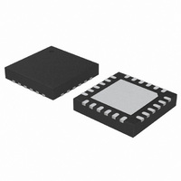
C8051F988-GM Silicon Laboratories Inc, C8051F988-GM Datasheet - Page 234

C8051F988-GM
Manufacturer Part Number
C8051F988-GM
Description
IC MCU 8BIT 4KB FLASH 24QFN
Manufacturer
Silicon Laboratories Inc
Series
C8051F9xxr
Specifications of C8051F988-GM
Program Memory Type
FLASH
Program Memory Size
4KB (4K x 8)
Package / Case
24-UQFN Exposed Pad, 24-HUQFN
Core Processor
8051
Core Size
8-Bit
Speed
25MHz
Connectivity
SMBus (2-Wire/I²C), SPI, UART/USART
Peripherals
Brown-out Detect/Reset, POR, PWM, Temp Sensor, WDT
Number Of I /o
17
Ram Size
512 x 8
Voltage - Supply (vcc/vdd)
1.8 V ~ 3.6 V
Data Converters
A/D 10x10b
Oscillator Type
Internal
Operating Temperature
-40°C ~ 85°C
Processor Series
C8051F9x
Core
8051
Data Ram Size
512 B
Interface Type
I2C, SMBus, Enhanced UART, Enhanced SPI
Maximum Clock Frequency
7 KHz
Number Of Programmable I/os
17
Number Of Timers
4
Operating Supply Voltage
2.4 V
Maximum Operating Temperature
+ 85 C
Mounting Style
SMD/SMT
3rd Party Development Tools
PK51, CA51, A51, ULINK2
Development Tools By Supplier
C8051F996DK
Minimum Operating Temperature
- 40 C
On-chip Adc
10 bit, 10 Channel
On-chip Dac
10 bit, 4 Channel
Lead Free Status / RoHS Status
Lead free / RoHS Compliant
Eeprom Size
-
Lead Free Status / Rohs Status
Lead free / RoHS Compliant
Other names
336-1959-5
- Current page: 234 of 322
- Download datasheet (3Mb)
C8051F99x-C8051F98x
22.1. Supporting Documents
It is assumed the reader is familiar with or has access to the following supporting documents:
22.2. SMBus Configuration
Figure 22.2 shows a typical SMBus configuration. The SMBus specification allows any recessive voltage
between 3.0 V and 5.0 V; different devices on the bus may operate at different voltage levels.
Note: The port pins on C8051F99x-C8051F98x devices are not 5 V tolerant, therefore, the device may only be used
The bi-directional SCL (serial clock) and SDA (serial data) lines must be connected to a positive power
supply voltage through a pullup resistor or similar circuit. Every device connected to the bus must have an
open-drain or open-collector output for both the SCL and SDA lines, so that both are pulled high (recessive
state) when the bus is free. The maximum number of devices on the bus is limited only by the requirement
that the rise and fall times on the bus not exceed 300 ns and 1000 ns, respectively.
234
The I
The I
System Management Bus Specification—Version 1.1, SBS Implementers Forum.
in SMBus networks where the supply voltage does not exceed V
2
2
VDD = 3 V
C-Bus and How to Use It (including specifications), Philips Semiconductor.
C-Bus Specification—Version 2.0, Philips Semiconductor.
Figure 22.2. Typical SMBus Configuration
VDD = 3 V
Master
Device
Rev. 1.0
VDD = 3 V
Device 1
Slave
DD
.
VDD = 3 V
Device 2
Slave
SDA
SCL
Related parts for C8051F988-GM
Image
Part Number
Description
Manufacturer
Datasheet
Request
R
Part Number:
Description:
SMD/C°/SINGLE-ENDED OUTPUT SILICON OSCILLATOR
Manufacturer:
Silicon Laboratories Inc
Part Number:
Description:
Manufacturer:
Silicon Laboratories Inc
Datasheet:
Part Number:
Description:
N/A N/A/SI4010 AES KEYFOB DEMO WITH LCD RX
Manufacturer:
Silicon Laboratories Inc
Datasheet:
Part Number:
Description:
N/A N/A/SI4010 SIMPLIFIED KEY FOB DEMO WITH LED RX
Manufacturer:
Silicon Laboratories Inc
Datasheet:
Part Number:
Description:
N/A/-40 TO 85 OC/EZLINK MODULE; F930/4432 HIGH BAND (REV E/B1)
Manufacturer:
Silicon Laboratories Inc
Part Number:
Description:
EZLink Module; F930/4432 Low Band (rev e/B1)
Manufacturer:
Silicon Laboratories Inc
Part Number:
Description:
I°/4460 10 DBM RADIO TEST CARD 434 MHZ
Manufacturer:
Silicon Laboratories Inc
Part Number:
Description:
I°/4461 14 DBM RADIO TEST CARD 868 MHZ
Manufacturer:
Silicon Laboratories Inc
Part Number:
Description:
I°/4463 20 DBM RFSWITCH RADIO TEST CARD 460 MHZ
Manufacturer:
Silicon Laboratories Inc
Part Number:
Description:
I°/4463 20 DBM RADIO TEST CARD 868 MHZ
Manufacturer:
Silicon Laboratories Inc
Part Number:
Description:
I°/4463 27 DBM RADIO TEST CARD 868 MHZ
Manufacturer:
Silicon Laboratories Inc
Part Number:
Description:
I°/4463 SKYWORKS 30 DBM RADIO TEST CARD 915 MHZ
Manufacturer:
Silicon Laboratories Inc
Part Number:
Description:
N/A N/A/-40 TO 85 OC/4463 RFMD 30 DBM RADIO TEST CARD 915 MHZ
Manufacturer:
Silicon Laboratories Inc
Part Number:
Description:
I°/4463 20 DBM RADIO TEST CARD 169 MHZ
Manufacturer:
Silicon Laboratories Inc


