C8051F988-GM Silicon Laboratories Inc, C8051F988-GM Datasheet - Page 314
C8051F988-GM
Manufacturer Part Number
C8051F988-GM
Description
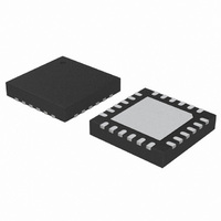
IC MCU 8BIT 4KB FLASH 24QFN
Manufacturer
Silicon Laboratories Inc
Series
C8051F9xxr
Specifications of C8051F988-GM
Program Memory Type
FLASH
Program Memory Size
4KB (4K x 8)
Package / Case
24-UQFN Exposed Pad, 24-HUQFN
Core Processor
8051
Core Size
8-Bit
Speed
25MHz
Connectivity
SMBus (2-Wire/I²C), SPI, UART/USART
Peripherals
Brown-out Detect/Reset, POR, PWM, Temp Sensor, WDT
Number Of I /o
17
Ram Size
512 x 8
Voltage - Supply (vcc/vdd)
1.8 V ~ 3.6 V
Data Converters
A/D 10x10b
Oscillator Type
Internal
Operating Temperature
-40°C ~ 85°C
Processor Series
C8051F9x
Core
8051
Data Ram Size
512 B
Interface Type
I2C, SMBus, Enhanced UART, Enhanced SPI
Maximum Clock Frequency
7 KHz
Number Of Programmable I/os
17
Number Of Timers
4
Operating Supply Voltage
2.4 V
Maximum Operating Temperature
+ 85 C
Mounting Style
SMD/SMT
3rd Party Development Tools
PK51, CA51, A51, ULINK2
Development Tools By Supplier
C8051F996DK
Minimum Operating Temperature
- 40 C
On-chip Adc
10 bit, 10 Channel
On-chip Dac
10 bit, 4 Channel
Lead Free Status / RoHS Status
Lead free / RoHS Compliant
Eeprom Size
-
Lead Free Status / Rohs Status
Lead free / RoHS Compliant
Other names
336-1959-5


C8051F99x-C8051F98x
SFR Definition 26.4. PCA0CPMn: PCA Capture/Compare Mode
SFR Address, Page: PCA0CPM0 = 0xDA
314
Note: When the WDTE bit is set to 1, the PCA0CPM5 register cannot be modified, and module 5 acts as the
Name
Reset
Bit
Type
7
6
5
4
3
2
1
0
Bit
PWM16n 16-bit Pulse Width Modulation Enable.
watchdog timer. To change the contents of the PCA0CPM5 register or the function of module 5, the Watchdog
Timer must be disabled.
ECOMn
CAPNn
CAPPn
ECCFn
PWMn
Name
TOGn
MATn
PWM16n
R/W
7
0
This bit enables 16-bit mode when Pulse Width Modulation mode is enabled.
0: 8 to 11-bit PWM selected.
1: 16-bit PWM selected.
Comparator Function Enable.
This bit enables the comparator function for PCA module n when set to 1.
Capture Positive Function Enable.
This bit enables the positive edge capture for PCA module n when set to 1.
Capture Negative Function Enable.
This bit enables the negative edge capture for PCA module n when set to 1.
Match Function Enable.
This bit enables the match function for PCA module n when set to 1. When enabled,
matches of the PCA counter with a module's capture/compare register cause the CCFn
bit in PCA0MD register to be set to logic 1.
Toggle Function Enable.
This bit enables the toggle function for PCA module n when set to 1. When enabled,
matches of the PCA counter with a module's capture/compare register cause the logic
level on the CEXn pin to toggle. If the PWMn bit is also set to logic 1, the module oper-
ates in Frequency Output Mode.
Pulse Width Modulation Mode Enable.
This bit enables the PWM function for PCA module n when set to 1. When enabled, a
pulse width modulated signal is output on the CEXn pin. 8 to 11-bit PWM is used if
PWM16n is cleared; 16-bit mode is used if PWM16n is set to logic 1. If the TOGn bit is
also set, the module operates in Frequency Output Mode.
Capture/Compare Flag Interrupt Enable.
This bit sets the masking of the Capture/Compare Flag (CCFn) interrupt.
0: Disable CCFn interrupts.
1: Enable a Capture/Compare Flag interrupt request when CCFn is set.
ECOMn
R/W
6
0
CAPPn
R/W
5
0
,
0x0; PCA0CPM1 = 0xDB
CAPNn
R/W
Rev. 1.0
4
0
Function
MATn
R/W
3
0
,
0x0; PCA0CPM2 = 0xDC, 0x0
TOGn
R/W
2
0
PWMn
R/W
1
0
ECCFn
R/W
0
0
Related parts for C8051F988-GM
Image
Part Number
Description
Manufacturer
Datasheet
Request
R

Part Number:
Description:
SMD/C°/SINGLE-ENDED OUTPUT SILICON OSCILLATOR
Manufacturer:
Silicon Laboratories Inc
Part Number:
Description:
Manufacturer:
Silicon Laboratories Inc
Datasheet:
Part Number:
Description:
N/A N/A/SI4010 AES KEYFOB DEMO WITH LCD RX
Manufacturer:
Silicon Laboratories Inc
Datasheet:
Part Number:
Description:
N/A N/A/SI4010 SIMPLIFIED KEY FOB DEMO WITH LED RX
Manufacturer:
Silicon Laboratories Inc
Datasheet:
Part Number:
Description:
N/A/-40 TO 85 OC/EZLINK MODULE; F930/4432 HIGH BAND (REV E/B1)
Manufacturer:
Silicon Laboratories Inc
Part Number:
Description:
EZLink Module; F930/4432 Low Band (rev e/B1)
Manufacturer:
Silicon Laboratories Inc
Part Number:
Description:
I°/4460 10 DBM RADIO TEST CARD 434 MHZ
Manufacturer:
Silicon Laboratories Inc
Part Number:
Description:
I°/4461 14 DBM RADIO TEST CARD 868 MHZ
Manufacturer:
Silicon Laboratories Inc
Part Number:
Description:
I°/4463 20 DBM RFSWITCH RADIO TEST CARD 460 MHZ
Manufacturer:
Silicon Laboratories Inc
Part Number:
Description:
I°/4463 20 DBM RADIO TEST CARD 868 MHZ
Manufacturer:
Silicon Laboratories Inc
Part Number:
Description:
I°/4463 27 DBM RADIO TEST CARD 868 MHZ
Manufacturer:
Silicon Laboratories Inc
Part Number:
Description:
I°/4463 SKYWORKS 30 DBM RADIO TEST CARD 915 MHZ
Manufacturer:
Silicon Laboratories Inc
Part Number:
Description:
N/A N/A/-40 TO 85 OC/4463 RFMD 30 DBM RADIO TEST CARD 915 MHZ
Manufacturer:
Silicon Laboratories Inc
Part Number:
Description:
I°/4463 20 DBM RADIO TEST CARD 169 MHZ
Manufacturer:
Silicon Laboratories Inc