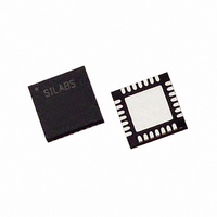
C8051F311-GM Silicon Laboratories Inc, C8051F311-GM Datasheet - Page 52

C8051F311-GM
Manufacturer Part Number
C8051F311-GM
Description
IC 8051 MCU 16K FLASH 28MLP
Manufacturer
Silicon Laboratories Inc
Series
C8051F31xr
Datasheets
1.C8051F310-TB.pdf
(228 pages)
2.C8051F311-GM.pdf
(2 pages)
3.C8051F310-GQ.pdf
(218 pages)
Specifications of C8051F311-GM
Program Memory Type
FLASH
Program Memory Size
16KB (16K x 8)
Package / Case
28-VQFN Exposed Pad, 28-HVQFN, 28-SQFN, 28-DHVQFN
Core Processor
8051
Core Size
8-Bit
Speed
25MHz
Connectivity
SMBus (2-Wire/I²C), SPI, UART/USART
Peripherals
POR, PWM, Temp Sensor, WDT
Number Of I /o
25
Ram Size
1.25K x 8
Voltage - Supply (vcc/vdd)
2.7 V ~ 3.6 V
Data Converters
A/D 17x10b
Oscillator Type
Internal
Operating Temperature
-40°C ~ 85°C
Processor Series
C8051F3x
Core
8051
Data Bus Width
8 bit
Data Ram Size
1.25 KB
Interface Type
I2C, SMBus, SPI, UART
Maximum Clock Frequency
25 MHz
Number Of Programmable I/os
25
Number Of Timers
4 bit
Operating Supply Voltage
2.7 V to 3.6 V
Maximum Operating Temperature
+ 85 C
Mounting Style
SMD/SMT
3rd Party Development Tools
PK51, CA51, A51, ULINK2
Development Tools By Supplier
C8051F310DK
Minimum Operating Temperature
- 40 C
On-chip Adc
10 bit, 17 Channel
No. Of I/o's
25
Ram Memory Size
1280Byte
Cpu Speed
25MHz
No. Of Timers
4
Rohs Compliant
Yes
Package
24QFN EP
Device Core
8051
Family Name
C8051F31x
Maximum Speed
25 MHz
Lead Free Status / RoHS Status
Lead free / RoHS Compliant
For Use With
770-1006 - ISP 4PORT FOR SILABS C8051F MCU336-1446 - ADAPTER PROGRAM TOOLSTICK F311336-1253 - DEV KIT FOR C8051F310/F311
Eeprom Size
-
Lead Free Status / Rohs Status
Lead free / RoHS Compliant
Other names
336-1254
Available stocks
Company
Part Number
Manufacturer
Quantity
Price
Part Number:
C8051F311-GM
Manufacturer:
SILICONLABS/芯科
Quantity:
20 000
Part Number:
C8051F311-GMR
Manufacturer:
SILICON LABS/芯科
Quantity:
20 000
C8051F310/1/2/3/4/5/6/7
Inputs are measured from ‘0’ to VREF * 1023/1024. Example codes are shown below for both right-justified
and left-justified data. Unused bits in the ADC0H and ADC0L registers are set to ‘0’.
When in Differential Mode, conversion codes are represented as 10-bit signed 2’s complement numbers.
Inputs are measured from -VREF to VREF * 511/512. Example codes are shown below for both right-justi-
fied and left-justified data. For right-justified data, the unused MSBs of ADC0H are a sign-extension of the
data word. For left-justified data, the unused LSBs in the ADC0L register are set to ‘0’.
Important Note About ADC0 Input Configuration: Port pins selected as ADC0 inputs should be config-
ured as analog inputs, and should be skipped by the Digital Crossbar. To configure a Port pin for analog
input, set to ‘0’ the corresponding bit in register PnMDIN (for n = 0,1,2,3). To force the Crossbar to skip a
Port pin, set to ‘1’ the corresponding bit in register PnSKIP (for n = 0,1,2). See
Output” on page 129
5.2.
The typical temperature sensor transfer function is shown in Figure 5.2. The output voltage (V
positive ADC input when the temperature sensor is selected by bits AMX0P4-0 in register AMX0P.
52
VREF x 1023/1024
VREF x 512/1024
VREF x 256/1024
–VREF x 256/512
VREF x 256/512
VREF x 511/512
Temperature Sensor
Input Voltage
Input Voltage
–VREF
0
0
Figure 5.2. Typical Temperature Sensor Transfer Function
for more Port I/O configuration details.
1200
1100
1000
(mV)
900
800
700
-50
Right-Justified ADC0H:ADC0L
Right-Justified ADC0H:ADC0L
(AD0LJST = 0)
(AD0LJST = 0)
0
0x03FF
0x0200
0x0100
0x0000
0x01FF
0xFE00
0x0100
0x0000
0xFF00
Rev. 1.7
V
TEMP
50
= 3.35*(TEMP
C
100
) + 897 mV
Left-Justified ADC0H:ADC0L
Left-Justified ADC0H:ADC0L
(Celsius)
(AD0LJST = 1)
(AD0LJST = 1)
Section “13. Port Input/
0xFFC0
0x8000
0x4000
0x0000
0x7FC0
0xC000
0x4000
0x0000
0x8000
TEMP
) is the


