MCF52213CAE50 Freescale Semiconductor, MCF52213CAE50 Datasheet - Page 9
MCF52213CAE50
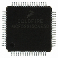
Manufacturer Part Number
MCF52213CAE50
Description
IC MCU 32BIT 128K FLASH 64-LQFP
Manufacturer
Freescale Semiconductor
Series
MCF5221xr
Datasheet
1.MCF52213CAE50.pdf
(56 pages)
Specifications of MCF52213CAE50
Core Processor
Coldfire V2
Core Size
32-Bit
Speed
50MHz
Connectivity
I²C, SPI, UART/USART, USB OTG
Peripherals
DMA, LVD, POR, PWM, WDT
Number Of I /o
56
Program Memory Size
128KB (128K x 8)
Program Memory Type
FLASH
Ram Size
8K x 8
Voltage - Supply (vcc/vdd)
3 V ~ 3.6 V
Data Converters
A/D 8x12b
Oscillator Type
Internal
Operating Temperature
-40°C ~ 85°C
Package / Case
64-LQFP
Processor Series
MCF522x
Core
ColdFire V2
Data Bus Width
32 bit
Data Ram Size
8 KB
Interface Type
I2C, QSPI, UART
Maximum Clock Frequency
50 MHz
Number Of Programmable I/os
43
Number Of Timers
18
Maximum Operating Temperature
+ 85 C
Mounting Style
SMD/SMT
3rd Party Development Tools
JLINK-CF-BDM26, EWCF
Development Tools By Supplier
M52210DEMO, M52211EVB
Minimum Operating Temperature
- 40 C
On-chip Adc
12 bit, 8 Channel
A/d Bit Size
12 bit
A/d Channels Available
8
Height
1.4 mm
Length
10 mm
Supply Voltage (max)
3.6 V
Supply Voltage (min)
3 V
Width
10 mm
For Use With
M52210DEMO - BOARD DEV MCF5221X LOW COST
Lead Free Status / RoHS Status
Lead free / RoHS Compliant
Eeprom Size
-
Lead Free Status / Rohs Status
Details
Available stocks
Company
Part Number
Manufacturer
Quantity
Price
Company:

Part Number:
MCF52213CAE50
Manufacturer:
Freescale Semiconductor
Quantity:
10 000


Family Configurations
The full debug/trace interface is available only on the 100-pin packages. However, every product features the dedicated debug
serial communication channel (DSI, DSO, DSCLK) and the ALLPST signal.
1.2.4
The processor supports circuit board test strategies based on the Test Technology Committee of IEEE and the Joint Test Action
Group (JTAG). The test logic includes a test access port (TAP) consisting of a 16-state controller, an instruction register, and
three test registers (a 1-bit bypass register, a 256-bit boundary-scan register, and a 32-bit ID register). The boundary scan register
links the device’s pins into one shift register. Test logic, implemented using static logic design, is independent of the device
system logic.
The device implementation can:
1.2.5
1.2.5.1
The dual-ported SRAM module provides a general-purpose 8- or 16-Kbyte memory block that the ColdFire core can access in
a single cycle. The location of the memory block can be set to any 8- or 16-Kbyte boundary within the 4-Gbyte address space.
This memory is ideal for storing critical code or data structures and for use as the system stack. Because the SRAM module is
physically connected to the processor's high-speed local bus, it can quickly service core-initiated accesses or
memory-referencing commands from the debug module.
The SRAM module is also accessible by the DMA. The dual-ported nature of the SRAM makes it ideal for implementing
applications with double-buffer schemes, where the processor and a DMA device operate in alternate regions of the SRAM to
maximize system performance.
1.2.5.2
The ColdFire flash module (CFM) is a non-volatile memory (NVM) module that connects to the processor’s high-speed local
bus. The CFM is constructed with up to four banks of 16-Kbyte16-bit flash memory arrays to generate up to 128 Kbytes of
32-bit flash memory. These electrically erasable and programmable arrays serve as non-volatile program and data memory. The
flash memory is ideal for program and data storage for single-chip applications, allowing for field reprogramming without
requiring an external high voltage source. The CFM interfaces to the ColdFire core through an optimized read-only memory
controller that supports interleaved accesses from the 2-cycle flash memory arrays. A backdoor mapping of the flash memory
is used for all program, erase, and verify operations, as well as providing a read datapath for the DMA. Flash memory may also
be programmed via the EzPort, which is a serial flash memory programming interface that allows the flash memory to be read,
erased and programmed by an external controller in a format compatible with most SPI bus flash memory chips.
1.2.6
The device incorporates several low-power modes of operation entered under program control and exited by several external
trigger events. An integrated power-on reset (POR) circuit monitors the input supply and forces an MCU reset as the supply
voltage rises. The low voltage detector (LVD) monitors the supply voltage and is configurable to force a reset or interrupt
condition if it falls below the LVD trip point. The RAM standby switch provides power to RAM when the supply voltage to the
chip falls below the standby battery voltage.
9
•
•
•
•
•
Perform boundary-scan operations to test circuit board electrical continuity
Sample system pins during operation and transparently shift out the result in the boundary scan register
Bypass the device for a given circuit board test by effectively reducing the boundary-scan register to a single bit
Disable the output drive to pins during circuit-board testing
Drive output pins to stable levels
JTAG
On-Chip Memories
Power Management
SRAM
Flash Memory
MCF52211 ColdFire Microcontroller, Rev. 2
Freescale Semiconductor
Related parts for MCF52213CAE50
Image
Part Number
Description
Manufacturer
Datasheet
Request
R

Part Number:
Description:
Manufacturer:
Freescale Semiconductor, Inc
Datasheet:
Part Number:
Description:
Manufacturer:
Freescale Semiconductor, Inc
Datasheet:
Part Number:
Description:
Manufacturer:
Freescale Semiconductor, Inc
Datasheet:
Part Number:
Description:
Manufacturer:
Freescale Semiconductor, Inc
Datasheet:
Part Number:
Description:
Manufacturer:
Freescale Semiconductor, Inc
Datasheet:
Part Number:
Description:
Manufacturer:
Freescale Semiconductor, Inc
Datasheet:
Part Number:
Description:
Manufacturer:
Freescale Semiconductor, Inc
Datasheet:
Part Number:
Description:
Manufacturer:
Freescale Semiconductor, Inc
Datasheet:
Part Number:
Description:
Manufacturer:
Freescale Semiconductor, Inc
Datasheet:
Part Number:
Description:
Manufacturer:
Freescale Semiconductor, Inc
Datasheet:
Part Number:
Description:
Manufacturer:
Freescale Semiconductor, Inc
Datasheet:
Part Number:
Description:
Manufacturer:
Freescale Semiconductor, Inc
Datasheet:
Part Number:
Description:
Manufacturer:
Freescale Semiconductor, Inc
Datasheet:
Part Number:
Description:
Manufacturer:
Freescale Semiconductor, Inc
Datasheet:
Part Number:
Description:
Manufacturer:
Freescale Semiconductor, Inc
Datasheet: