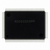
M30622SAFP#U5 Renesas Electronics America, M30622SAFP#U5 Datasheet - Page 371

M30622SAFP#U5
Manufacturer Part Number
M30622SAFP#U5
Description
IC M16C MPU ROMLESS 100QFP
Manufacturer
Renesas Electronics America
Series
M16C™ M16C/60r
Datasheets
1.QSK-62P_PLUS.pdf
(103 pages)
2.M30622SAFPU5.pdf
(277 pages)
3.M30622SAFPU5.pdf
(617 pages)
4.M30622SAFPU5.pdf
(308 pages)
Specifications of M30622SAFP#U5
Core Processor
M16C/60
Core Size
16-Bit
Speed
16MHz
Connectivity
SIO, UART/USART
Peripherals
DMA, PWM, WDT
Number Of I /o
50
Program Memory Type
ROMless
Ram Size
3K x 8
Voltage - Supply (vcc/vdd)
4.2 V ~ 5.5 V
Data Converters
A/D 10x10b, D/A 2x8b
Oscillator Type
Internal
Operating Temperature
-20°C ~ 85°C
Package / Case
100-QFP
For Use With
867-1000 - KIT QUICK START RENESAS 62PM3062PT3-CPE-3 - EMULATOR COMPACT M16C/62P/30P
Lead Free Status / RoHS Status
Lead free / RoHS Compliant
Eeprom Size
-
Program Memory Size
-
Available stocks
Company
Part Number
Manufacturer
Quantity
Price
- QSK-62P_PLUS PDF datasheet
- M30622SAFPU5 PDF datasheet #2
- M30622SAFPU5 PDF datasheet #3
- M30622SAFPU5 PDF datasheet #4
- Current page: 371 of 617
- Download datasheet (9Mb)
Clock-Synchronous Serial I/O
2-52
2.4 Clock-Synchronous Serial I/O Usage
2.4.1 Overview of the clock-synchronous serial I/O usage
Clock-synchronous serial I/O carries out 8-bit data communications in synchronization with the clock. The
following is an overview of the clock-synchronous serial I/O usage.
(1) Transmission/reception format
(2) Transfer rate
(3) Error detection
(4) How to deal with an error
(5) Function selection
8-bit data
If the internal clock is selected as the transfer clock, the divide-by-2 frequency, resulting from the bit
rate generator division, becomes the transfer rate. The bit rate generator count source can be se-
lected from the following: f
clock by 1, 8, and 32 respectively.
Furthermore, if an external clock is selected as the transfer clock, the clock frequency input to the CLK
pin becomes the transfer rate.
Only overrun error can be detected. Overrun error is an error that occurs when the next data is made
ready before the reception buffer register is read.
When receiving data, read an error flag and reception data simultaneously to determine which error
has occurred. If the data read is erroneous, initialize the error flag and the UARTi receive buffer
register, then receive the data again.
To initialize the UARTi receive buffer register
To set the UARTi transmit buffer register again
For clock-synchronous serial I/O, the following functions can be selected:
(a) CTS/RTS function
1. Set the receive enable bit to “0” (disable reception).
2. Set the serial I/O mode select bit to “000
3. Set the serial I/O mode select bit.
4. Set the receive enable bit to “1” again (enable reception).
To transmit data again due to an error on the reception side, set the UARTi transmit buffer register
again, then transmit the data again.
1. Set the serial I/O mode select bits to “000
2. Set the serial I/O mode select bits again.
3. Set the transmit enable bit to “1” (enable transmission), then set transmission data in the UARTi
In the CTS function, an external IC can start transmission/reception by inputting an “H” level to the
_______
CTS pin. The CTS pin input level is detected when transmission/reception starts. Therefore, if the
level is set to “L” during transmission/reception, it will stop from the next data.
The RTS function informs an external IC that RTS is reception-ready and has changed to “L”. RTS
goes to “H” at the falling edge of the transfer clock.
_______ _______
transmit buffer register.
_______
_______
_______
1
, f
8
, and f
32
. Clocks f
2
” (invalid serial I/O).
2
” (invalidate serial I/O).
_______
1
, f
8
, and f
32
are derived by dividing the CPU’s main
SINGLE-CHIP 16-BIT CMOS MICROCOMPUTER
M16C / 62A Group
Mitsubishi microcomputers
_______
Related parts for M30622SAFP#U5
Image
Part Number
Description
Manufacturer
Datasheet
Request
R

Part Number:
Description:
KIT STARTER FOR M16C/29
Manufacturer:
Renesas Electronics America
Datasheet:

Part Number:
Description:
KIT STARTER FOR R8C/2D
Manufacturer:
Renesas Electronics America
Datasheet:

Part Number:
Description:
R0K33062P STARTER KIT
Manufacturer:
Renesas Electronics America
Datasheet:

Part Number:
Description:
KIT STARTER FOR R8C/23 E8A
Manufacturer:
Renesas Electronics America
Datasheet:

Part Number:
Description:
KIT STARTER FOR R8C/25
Manufacturer:
Renesas Electronics America
Datasheet:

Part Number:
Description:
KIT STARTER H8S2456 SHARPE DSPLY
Manufacturer:
Renesas Electronics America
Datasheet:

Part Number:
Description:
KIT STARTER FOR R8C38C
Manufacturer:
Renesas Electronics America
Datasheet:

Part Number:
Description:
KIT STARTER FOR R8C35C
Manufacturer:
Renesas Electronics America
Datasheet:

Part Number:
Description:
KIT STARTER FOR R8CL3AC+LCD APPS
Manufacturer:
Renesas Electronics America
Datasheet:

Part Number:
Description:
KIT STARTER FOR RX610
Manufacturer:
Renesas Electronics America
Datasheet:

Part Number:
Description:
KIT STARTER FOR R32C/118
Manufacturer:
Renesas Electronics America
Datasheet:

Part Number:
Description:
KIT DEV RSK-R8C/26-29
Manufacturer:
Renesas Electronics America
Datasheet:

Part Number:
Description:
KIT STARTER FOR SH7124
Manufacturer:
Renesas Electronics America
Datasheet:

Part Number:
Description:
KIT STARTER FOR H8SX/1622
Manufacturer:
Renesas Electronics America
Datasheet:

Part Number:
Description:
KIT DEV FOR SH7203
Manufacturer:
Renesas Electronics America
Datasheet:


