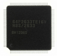
R5F61668RN50FPV Renesas Electronics America, R5F61668RN50FPV Datasheet - Page 57

R5F61668RN50FPV
Manufacturer Part Number
R5F61668RN50FPV
Description
IC H8SX/1668 MCU FLASH 144LQFP
Manufacturer
Renesas Electronics America
Series
H8® H8SX/1600r
Datasheet
1.R5F61668RN50FPV.pdf
(1506 pages)
Specifications of R5F61668RN50FPV
Core Processor
H8SX
Core Size
16/32-Bit
Speed
50MHz
Connectivity
EBI/EMI, I²C, IrDA, SCI, SmartCard, USB
Peripherals
DMA, LVD, POR, PWM, WDT
Number Of I /o
92
Program Memory Size
1MB (1M x 8)
Program Memory Type
FLASH
Ram Size
56K x 8
Voltage - Supply (vcc/vdd)
3 V ~ 3.6 V
Data Converters
A/D 8x10b; D/A 2x8b
Oscillator Type
External
Operating Temperature
-20°C ~ 75°C
Package / Case
144-LQFP
For Use With
R0K561668S000BE - KIT STARTER FOR H8SX/1668R0K561664S001BE - KIT STARTER FOR H8SX/1651HS0005KCU11H - EMULATOR E10A-USB H8S(X),SH2(A)
Lead Free Status / RoHS Status
Lead free / RoHS Compliant
Eeprom Size
-
Available stocks
Company
Part Number
Manufacturer
Quantity
Price
Company:
Part Number:
R5F61668RN50FPV
Manufacturer:
Renesas Electronics America
Quantity:
10 000
- Current page: 57 of 1506
- Download datasheet (9Mb)
1.4.3
Table 1.5
Classification
Power supply
Clock
Operating mode
control
System control
On-chip
emulator
Pin Functions
Pin Functions
Pin Name
V
V
V
PLLV
PLLV
DrV
DrV
XTAL
EXTAL
OSC1
OSC2
Bφ
SDRAMφ
MD3 to MD0 Input
MD_CLK
RES
STBY
EMLE
TRST
TMS
TDI
TCK
TDO
CC
CL
SS
CC
SS
CC
SS
I/O
Input
Input
Input
Input
Input
Input
Input
Input
Input
Input
Input
Output
Output
Input
Input
Input
Input
Input
Input
Input
Input
Output
Description
Power supply pins. Connect them to the system power supply.
Connect this pin to V
be placed close to the pin).
Ground pins. Connect them to the system power supply (0 V).
Power supply pin for the PLL circuit. Connect them to the system
power supply.
Ground pin for the PLL circuit.
Power supply pin for the on-chip USB transceiver. Connect this pin
to the system power supply.
Ground pin for the on-chip USB transceiver.
Pins for a crystal resonator. An external clock signal can be input
through the EXTAL pin. For an example of this connection, see
section 27, Clock Pulse Generator.
The 32.768 KH crystal resonator is connected to this pin.
The 32.768 KH crystal resonator is connected to this pin.
Outputs the system clock for external devices.
When connecting the synchronous DRAM, connect it to the CLK pin
of synchronous DRAM. For details, see section 9, Bus Controller
(BSC).
Pins for setting the operating mode. The signal levels on these pins
must not be changed during operation.
This pin changes the multiplication ratio of the clock oscillator. Do
not change values on this pin during operation.
Reset signal input pin. This LSI enters the reset state when this
signal goes low.
This LSI enters hardware standby mode when this signal goes low.
Input pin for the on-chip emulator enable signal. The signal level
should normally be fixed low.
On-chip emulator pins or boundary scan pins. When the EMLE pin is
driven high, these pins are dedicated for the on-chip emulator. When
the EMLE pin is driven low and to mode 3, these pins are dedicated
for the boundary scan mode.
SS
via a 0.1-µF capacitor (The capacitor should
Rev. 2.00 Sep. 24, 2008 Page 23 of 1468
Section 1 Overview
REJ09B0412-0200
Related parts for R5F61668RN50FPV
Image
Part Number
Description
Manufacturer
Datasheet
Request
R

Part Number:
Description:
KIT STARTER FOR M16C/29
Manufacturer:
Renesas Electronics America
Datasheet:

Part Number:
Description:
KIT STARTER FOR R8C/2D
Manufacturer:
Renesas Electronics America
Datasheet:

Part Number:
Description:
R0K33062P STARTER KIT
Manufacturer:
Renesas Electronics America
Datasheet:

Part Number:
Description:
KIT STARTER FOR R8C/23 E8A
Manufacturer:
Renesas Electronics America
Datasheet:

Part Number:
Description:
KIT STARTER FOR R8C/25
Manufacturer:
Renesas Electronics America
Datasheet:

Part Number:
Description:
KIT STARTER H8S2456 SHARPE DSPLY
Manufacturer:
Renesas Electronics America
Datasheet:

Part Number:
Description:
KIT STARTER FOR R8C38C
Manufacturer:
Renesas Electronics America
Datasheet:

Part Number:
Description:
KIT STARTER FOR R8C35C
Manufacturer:
Renesas Electronics America
Datasheet:

Part Number:
Description:
KIT STARTER FOR R8CL3AC+LCD APPS
Manufacturer:
Renesas Electronics America
Datasheet:

Part Number:
Description:
KIT STARTER FOR RX610
Manufacturer:
Renesas Electronics America
Datasheet:

Part Number:
Description:
KIT STARTER FOR R32C/118
Manufacturer:
Renesas Electronics America
Datasheet:

Part Number:
Description:
KIT DEV RSK-R8C/26-29
Manufacturer:
Renesas Electronics America
Datasheet:

Part Number:
Description:
KIT STARTER FOR SH7124
Manufacturer:
Renesas Electronics America
Datasheet:

Part Number:
Description:
KIT STARTER FOR H8SX/1622
Manufacturer:
Renesas Electronics America
Datasheet:

Part Number:
Description:
KIT DEV FOR SH7203
Manufacturer:
Renesas Electronics America
Datasheet:


