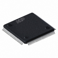
LPC2158FBD100,551 NXP Semiconductors, LPC2158FBD100,551 Datasheet - Page 13

LPC2158FBD100,551
Manufacturer Part Number
LPC2158FBD100,551
Description
IC ARM7 MCU FLASH 512K 100LQFP
Manufacturer
NXP Semiconductors
Series
LPC2100r
Datasheet
1.LPC2157FBD100551.pdf
(45 pages)
Specifications of LPC2158FBD100,551
Core Processor
ARM7
Core Size
16/32-Bit
Speed
60MHz
Connectivity
I²C, Microwire, SPI, SSI, SSP, UART/USART, USB
Peripherals
Brown-out Detect/Reset, DMA, LCD, POR, PWM, WDT
Number Of I /o
38
Program Memory Size
512KB (512K x 8)
Program Memory Type
FLASH
Ram Size
40K x 8
Voltage - Supply (vcc/vdd)
3 V ~ 3.6 V
Data Converters
A/D 14x10b; D/A 1x10b
Oscillator Type
Internal
Operating Temperature
-40°C ~ 85°C
Package / Case
100-LQFP
Processor Series
LPC21
Core
ARM7TDMI-S
Data Bus Width
32 bit
Data Ram Size
40 KB
Interface Type
I2C, SPI
Maximum Clock Frequency
25 MHz
Number Of Programmable I/os
38
Number Of Timers
2
Operating Supply Voltage
2.4 V to 3.6 V
Maximum Operating Temperature
+ 85 C
Mounting Style
SMD/SMT
3rd Party Development Tools
MDK-ARM, RL-ARM, ULINK2, LCD-DEMO-LPC2158
Development Tools By Supplier
OM11020
Minimum Operating Temperature
- 40 C
On-chip Adc
10 bit, 8 Channel
On-chip Dac
10 bit, 1 Channel
For Use With
568-4310 - EVAL BOARD LPC2158 W/LCD568-4297 - BOARD EVAL LPC21XX MCB2100622-1005 - USB IN-CIRCUIT PROG ARM7 LPC2K
Lead Free Status / RoHS Status
Lead free / RoHS Compliant
Eeprom Size
-
Lead Free Status / Rohs Status
Details
Other names
568-4691
935287349551
LPC2158FBD100-S
935287349551
LPC2158FBD100-S
Available stocks
Company
Part Number
Manufacturer
Quantity
Price
Company:
Part Number:
LPC2158FBD100,551
Manufacturer:
NXP Semiconductors
Quantity:
10 000
NXP Semiconductors
Table 3.
LPC2157_2158_1
Product data sheet
Symbol
P0[31]/UP_LED/
CONNECT
P1[0] to P1[31]
P1[16]
P1[17]
P1[25]/EXTIN0
P1[26]/RTCK
P1[27]/TDO
P1[28]/TDI
P1[29]/TCK
P1[30]/TMS
P1[31]/TRST
D+
D
RESET
XTAL1
XTAL2
RTCX1
RTCX2
V
SS
Pin description LPC2158
Pin
5
4
100
16
12
90
86
82
78
8
98
99
83
88
87
93
94
6, 13, 32,
39, 40,
85, 95
[6]
[6]
[6]
[6]
[6]
[6]
[6]
[6]
[6]
[7]
[7]
[8]
[9]
[9]
[9]
[9]
[6]
Type
O
O
O
I/O
I/O
I/O
I/O
I
I/O
I/O
I/O
O
I/O
I
I/O
I
I/O
I
I/O
I
I/O
I/O
I
O
I
I
O
I
…continued
Description
P0[31] — General purpose output only digital pin.
UP_LED — USB GoodLink LED indicator. It is LOW when device is configured
(non-control endpoints enabled). It is HIGH when the device is not configured
or during global suspend.
CONNECT — Signal used to switch an external 1.5 k resistor under the
software control. Used with the SoftConnect USB feature.
Important: This is an digital output only pin. This pin MUST NOT be externally
pulled LOW when RESET pin is LOW or the JTAG port will be disabled.
Port 1: Port 1 is a 32-bit bidirectional I/O port with individual direction controls
for each bit. The operation of port 1 pins depends upon the pin function
selected via the pin connect block. Pins 0 through 15 and 18 through 24 of
port 1 are not available.
P1[16] — General purpose input/output digital pin (GPIO).
P1[17] — General purpose input/output digital pin (GPIO).
P1[25] — General purpose input/output digital pin (GPIO).
EXTIN0 — External Trigger Input. Standard I/O with internal pull-up.
P1[26] — General purpose input/output digital pin (GPIO).
RTCK — Returned Test Clock output. Extra signal added to the JTAG port.
Assists debugger synchronization when processor frequency varies.
Bidirectional pin with internal pull-up.
Note: LOW on RTCK while RESET is LOW enables pins P1[31:26] to operate
as Debug port after reset.
P1[27] — General purpose input/output digital pin (GPIO).
TDO — Test Data out for JTAG interface.
P1[28] — General purpose input/output digital pin (GPIO).
TDI — Test Data in for JTAG interface.
P1[29] — General purpose input/output digital pin (GPIO).
TCK — Test Clock for JTAG interface.
P1[30] — General purpose input/output digital pin (GPIO).
TMS — Test Mode Select for JTAG interface.
P1[31] — General purpose input/output digital pin (GPIO).
TRST — Test Reset for JTAG interface.
USB bidirectional D+ line.
USB bidirectional D line.
External reset input: A LOW on this pin resets the device, causing I/O ports
and peripherals to take on their default states, and processor execution to
begin at address 0. TTL with hysteresis, 5 V tolerant.
Input from the oscillator amplifier.
Output to the oscillator circuit and internal clock generator circuits.
Input to the RTC oscillator circuit.
Output from the RTC oscillator circuit.
Ground: 0 V reference.
Rev. 01 — 15 October 2008
Single-chip 16-bit/32-bit microcontrollers
LPC2157/2158
© NXP B.V. 2008. All rights reserved.
13 of 45


