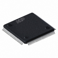
LPC2158FBD100,551 NXP Semiconductors, LPC2158FBD100,551 Datasheet - Page 28

LPC2158FBD100,551
Manufacturer Part Number
LPC2158FBD100,551
Description
IC ARM7 MCU FLASH 512K 100LQFP
Manufacturer
NXP Semiconductors
Series
LPC2100r
Datasheet
1.LPC2157FBD100551.pdf
(45 pages)
Specifications of LPC2158FBD100,551
Core Processor
ARM7
Core Size
16/32-Bit
Speed
60MHz
Connectivity
I²C, Microwire, SPI, SSI, SSP, UART/USART, USB
Peripherals
Brown-out Detect/Reset, DMA, LCD, POR, PWM, WDT
Number Of I /o
38
Program Memory Size
512KB (512K x 8)
Program Memory Type
FLASH
Ram Size
40K x 8
Voltage - Supply (vcc/vdd)
3 V ~ 3.6 V
Data Converters
A/D 14x10b; D/A 1x10b
Oscillator Type
Internal
Operating Temperature
-40°C ~ 85°C
Package / Case
100-LQFP
Processor Series
LPC21
Core
ARM7TDMI-S
Data Bus Width
32 bit
Data Ram Size
40 KB
Interface Type
I2C, SPI
Maximum Clock Frequency
25 MHz
Number Of Programmable I/os
38
Number Of Timers
2
Operating Supply Voltage
2.4 V to 3.6 V
Maximum Operating Temperature
+ 85 C
Mounting Style
SMD/SMT
3rd Party Development Tools
MDK-ARM, RL-ARM, ULINK2, LCD-DEMO-LPC2158
Development Tools By Supplier
OM11020
Minimum Operating Temperature
- 40 C
On-chip Adc
10 bit, 8 Channel
On-chip Dac
10 bit, 1 Channel
For Use With
568-4310 - EVAL BOARD LPC2158 W/LCD568-4297 - BOARD EVAL LPC21XX MCB2100622-1005 - USB IN-CIRCUIT PROG ARM7 LPC2K
Lead Free Status / RoHS Status
Lead free / RoHS Compliant
Eeprom Size
-
Lead Free Status / Rohs Status
Details
Other names
568-4691
935287349551
LPC2158FBD100-S
935287349551
LPC2158FBD100-S
Available stocks
Company
Part Number
Manufacturer
Quantity
Price
Company:
Part Number:
LPC2158FBD100,551
Manufacturer:
NXP Semiconductors
Quantity:
10 000
NXP Semiconductors
LPC2157_2158_1
Product data sheet
6.21.10 Data pointer
6.21.4.1 Internal clock
6.21.4 Oscillator
6.21.5 Timing
6.21.6 Display register
6.21.7 Segment outputs
6.21.8 Backplane outputs
6.21.9 Display RAM
An internal oscillator provides the clock signals for the internal logic of the LCD controller
and its LCD drive signals. After power-up, pin SDA must be HIGH to guarantee that the
clock starts.
The LCD controller timing controls the internal data flow of the device. This includes the
transfer of display data from the display RAM to the display segment outputs. The timing
also generates the LCD frame signal whose frequency is derived from the clock
frequency. The frame signal frequency is a fixed division of the clock frequency from either
the internal or an external clock.
Frame frequency = f
A display latch holds the display data while the corresponding multiplex signals are
generated. There is a one-to-one relationship between the data in the display latch, the
LCD segment outputs, and each column of the display RAM.
The LCD drive section includes 32 segment outputs S0 to S31. The segment output
signals are generated according to the multiplexed backplane signals and the display
latch data. When less than 32 segment outputs are required, the unused segment outputs
should be left open-circuit.
The LCD drive section has four backplane outputs BP0 to BP3. The backplane output
signals are generated in accordance with the selected LCD drive mode. If less than four
backplane outputs are required, the unused outputs can be left open-circuit. In the 1:3
multiplex drive mode, BP3 carries the same signal as BP1, therefore these two adjacent
outputs can be tied together to give enhanced drive capabilities. In the 1:2 multiplex drive
mode, BP0 and BP2, BP1 and BP3 respectively carry the same signals and may also be
paired to increase the drive capabilities. In the static drive mode the same signal is carried
by all four backplane outputs and they can be connected in parallel for very high drive
requirements.
The display RAM is a static 32
correspondence between the RAM addresses and the segment outputs, and between the
individual bits of a RAM word and the backplane outputs. The first RAM column
corresponds to the 32 segments for backplane 0 (BP0). In multiplexed LCD applications
the segment data of the second, third and fourth column of the display RAM are
time-multiplexed with BP1, BP2 and BP3 respectively.
The Display RAM is addressed using the data pointer. Either a single byte or a series of
display bytes may be loaded into any location of the display RAM.
osc(ctrl)LCD
Rev. 01 — 15 October 2008
/24.
4-bit RAM which stores LCD data. There is a one-to-one
Single-chip 16-bit/32-bit microcontrollers
LPC2157/2158
© NXP B.V. 2008. All rights reserved.
28 of 45


